Perovskite Solar Cell (PSC) Tutorial - Part D (Outputs & deeper understanding)
1. Electrical parameters
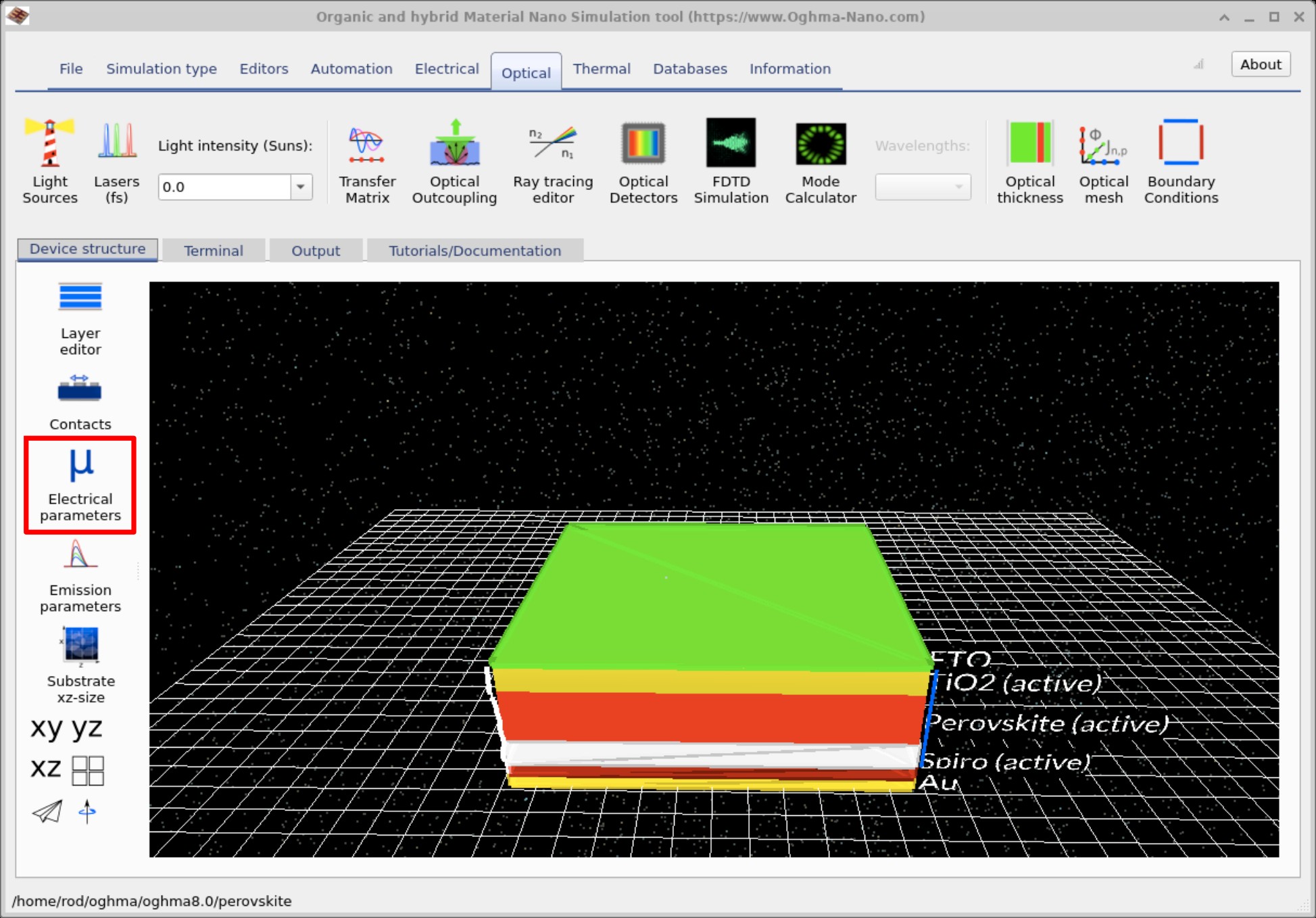
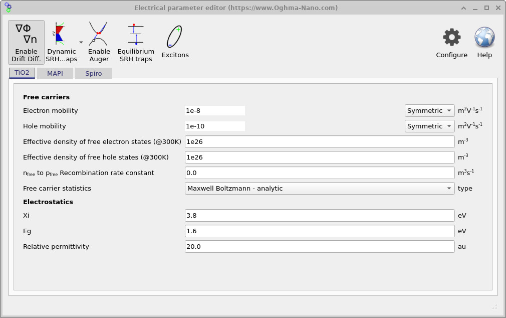
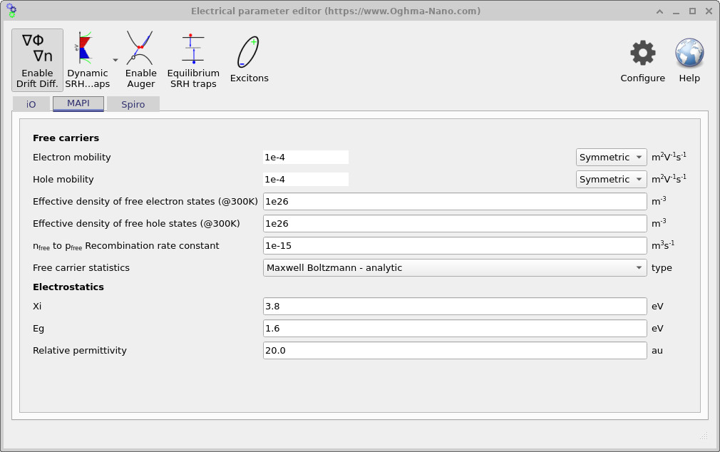
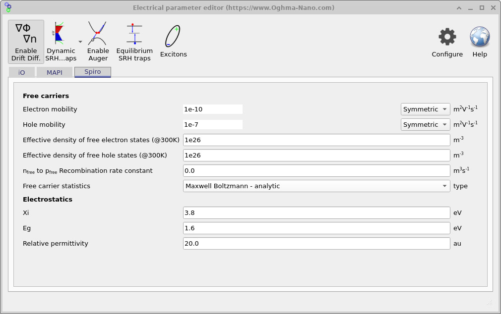
You can access the electrical parameter editor by clicking the Electrical parameters button in the main interface (see ??). This editor allows you to adjust mobilities, recombination constants, trap models, and other processes associated with active layers. Each active layer of the device is displayed in its own tab within the window. Examples for the Spiro, MAPI, and TiO₂ layers are shown in ??, ??, and ??. Any layer marked as active in the Layer editor will appear here.
The toolbar at the top enables or disables specific physical mechanisms — pressing a button switches the mechanism on:
- Drift–diffusion : Normally enabled for any active layer; only turn it off for insulating layers in a stack (e.g., OFET gate dielectrics) where no mobile charge is solved.
- Auger recombination: Rarely used in perovskite devices; mainly relevant at very high carrier densities (LEDs/lasers, concentrated illumination).
- Dynamic Shockley–Read–Hall (SRH) traps and Equilibrium SRH traps: Used to describe recombination via trap states; more commonly used in organic semiconductors but can also be applied to perovskites.
- Excitons: Exciton/geminate models for OPV and singlet/triplet models for OLEDs; generally not enabled for perovskite solar cells.
2. Bimolecular recombination in perovskites
In perovskite solar cells, recombination can occur through two main pathways: trap-assisted (Shockley–Read–Hall) and free-to-free (bimolecular) recombination. Trap-mediated recombination is often important, but in perovskites the traps are generally shallow (≈20 meV). Because carriers can easily escape from these traps, their overall effect can often be approximated by a simpler free-to-free recombination model.
R(x) = k · n(x) · p(x)
Here, R(x) is the recombination rate, k is the bimolecular rate constant, and n(x), p(x) are the local electron and hole densities. Increasing k shortens carrier lifetimes and reduces steady-state densities, while decreasing it allows carriers to persist longer in the device.
3. Mobility, recombination, lifetime, and the μτ product in perovskites
In perovskite solar cells, two of the most critical parameters for device performance are the carrier mobility (μ) and the free-to-free (bimolecular) recombination constant (k). In OghmaNano, these are set in the Electrical Parameter Editor: the Electron mobility and Hole mobility fields define μ, while the nfree → pfree recombination rate constant field defines k (see Free-to-free recombination).
Mobility controls how quickly carriers drift to the contacts: higher μ means carriers travel faster, reducing their chance of recombination. The recombination constant k sets the carrier lifetime (τ). Large values of k shorten τ, while smaller values extend it. A simplified relation is:
τ ≈ 1 / (k · n)
where n is the carrier concentration. This highlights why recombination rates matter so strongly in perovskites, which often operate under high carrier densities due to their excellent absorption. Small changes in k can dramatically alter τ and, therefore, the balance between recombination and extraction.
Together, mobility and lifetime form the μτ product (μ·τ), which expresses the average distance a carrier can travel before recombining. A larger μτ improves the probability that photogenerated carriers reach the contacts, boosting current and efficiency. In perovskites, high μτ values are one reason why these materials can achieve strong performance even with relatively thick active layers. Although μτ is not the only descriptor of device quality—factors like optical absorption, energy-level alignment, and contact selectivity also play major roles—it remains a valuable figure of merit for assessing transport–recombination balance.
4. S-shaped JV curves from bad contacts
In real perovskite solar cells, poorly performing contacts often lead to S-shaped JV curves. Instead of a smooth diode-like response, the curve shows a kink or plateau, which strongly suppresses current output. This behaviour indicates inefficient carrier extraction: photogenerated carriers build up at an interface because they cannot be transported efficiently through the adjacent transport layer. The resulting space charge and band bending hinder further extraction, giving rise to the S-shape.
In OghmaNano, this effect can be reproduced by deliberately reducing the carrier mobility of the electron transport layer (TiO₂) (see Figure 2) or the hole transport layer (Spiro) (see Figure 4). Lower mobilities make these layers act as transport bottlenecks, mimicking the effect of bad contacts.
📝 Check your understanding (Part E)
- In the Electrical Parameter Editor, which fields set (a) electron mobility, (b) hole mobility, and (c) the free-to-free recombination constant?
- Write the expression for the bimolecular recombination rate R(x) in terms of k, n(x), and p(x), and explain how this links to carrier lifetime (τ).
- What does the μτ product represent physically, and why is it particularly useful for assessing perovskite solar cells?
- Perovskite traps are typically shallow (~20 meV). Why can their recombination often be approximated using a free-to-free model rather than a full SRH trap model?
👉 Next steps:
- Continue to Part F: Contacts and VOC to explore how contact properties influence the open-circuit voltage of perovskite solar cells.
- Return to the perovskite solar cell simulation guide for the full tutorial overview.