Perovskite Solar Cell (PSC) Tutorial – Part D: Parasitic Components & Dark JV
1. Parasitic effects in perovskite devices
Drift–diffusion modelling gives a detailed picture of the perovskite absorber, where both electrons and holes are present and recombination, trapping, and photogeneration occur. However, real perovskite solar cells also show non-ideal behaviour caused by their transport layers, contacts, and fabrication imperfections. These effects appear as parasitic components that modify the JV curve.
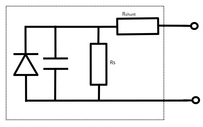
One of the most common parasitics is the series resistance (Rs), which comes from the finite conductivity of the transparent electrode (e.g. FTO), carrier transport layers such as TiO₂ or Spiro-OMeTAD, and even wiring and sheet resistance. It mainly affects the high-voltage region of the JV curve, where current begins to roll off, lowering the fill factor and reducing the maximum power point.
Another important loss is the shunt resistance (Rshunt). This represents leakage pathways that bypass the active perovskite, often caused by pinholes, roughness, incomplete coverage, or processing defects. In a JV plot, shunting appears as a flattened slope around 0 V, which reduces JSC, fill factor, and device stability.
These contributions are captured in a compact equivalent circuit model, shown in ??. Here the drift–diffusion diode (representing the perovskite) sits in parallel with Rshunt and in series with Rs. An optional capacitance term can be added to describe geometric capacitance, which becomes important in transient studies.
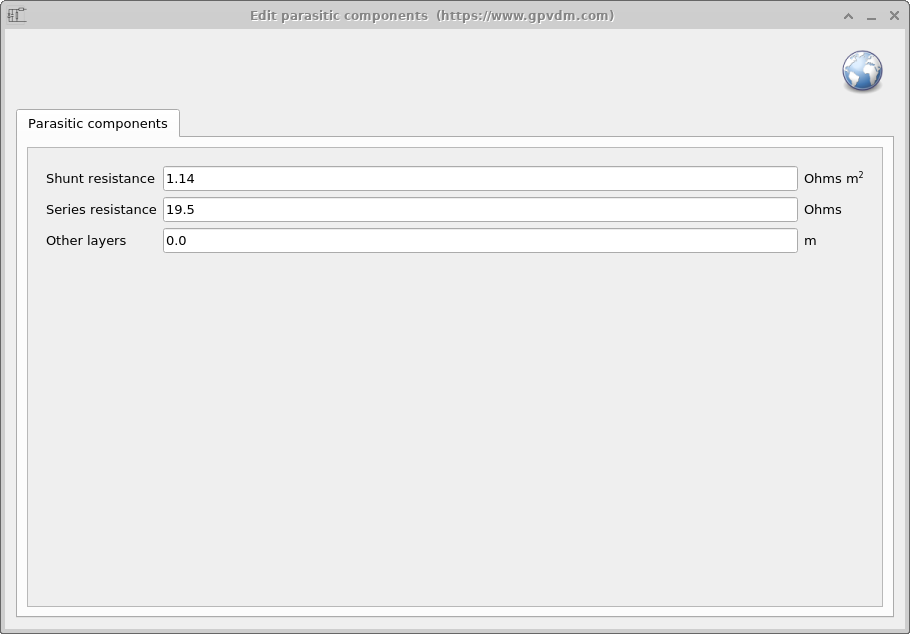
In OghmaNano, parasitics are edited through the Parasitic components editor, available under the Electrical ribbon (see ??). Shunt resistance is entered as an area-normalised value (Ω·m²), so that the effective leakage scales with device size. Series resistance is given as a lumped value in ohms (Ω), independent of area. Together, Rs and Rshunt allow you to reproduce the key non-idealities that real MAPbI₃ devices display in experiments.
2. Analysing perovskite devices in the dark
So far, every simulation has been performed under illumination with the AM1.5G spectrum. This makes sense if the goal is to predict power output, but solar-cell researchers know that dark JV curves often give deeper insight. Measuring or simulating a device without light removes the photocurrent and isolates the electronic losses of the stack. In many cases the dark curve is more revealing than the illuminated one when diagnosing why a perovskite cell falls short of its theoretical performance.
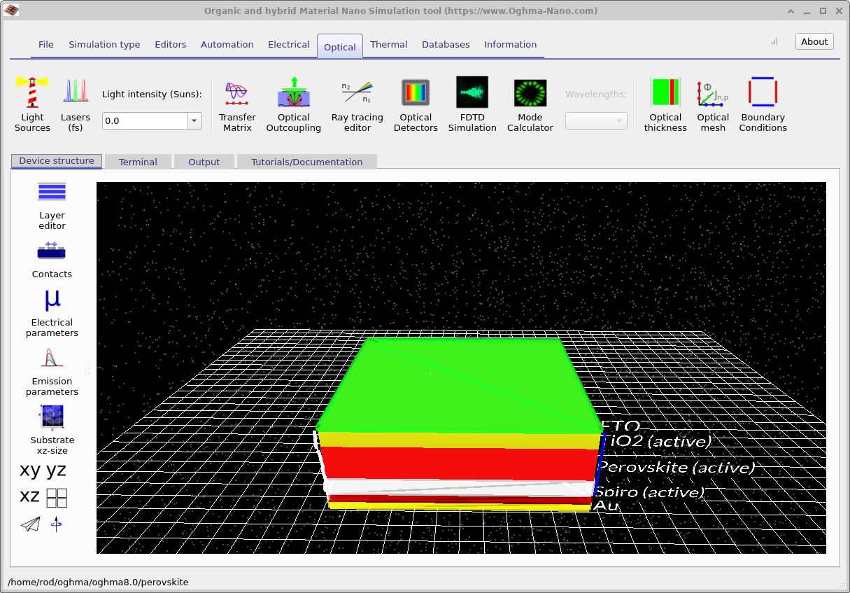
In this exercise you will extract Rshunt and Rs directly from a dark JV. To switch off illumination in OghmaNano, go to Optical ribbon → Light intensity (suns) and set the value to 0.0. The green photon markers in the 3D device panel disappear, confirming that the model is running under dark conditions (??).
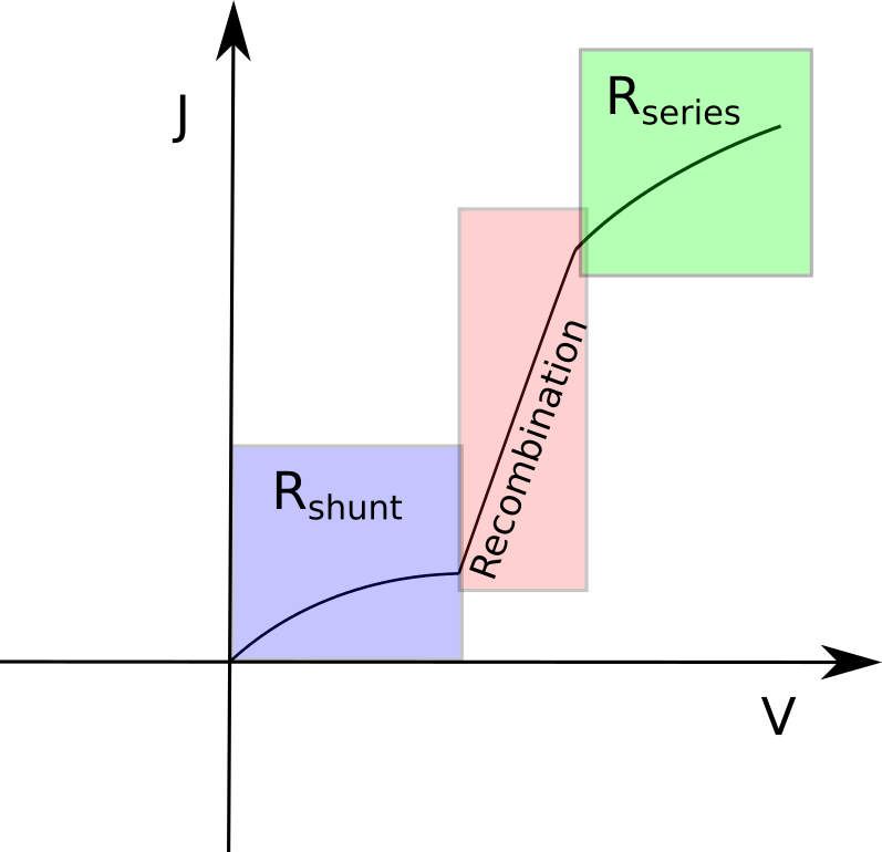
Now examine how parasitic resistances shape the curve. Start with Rshunt set very high (e.g. 1 MΩ·m²) and run a sweep. Then reduce it to a low value (e.g. 1 Ω·m²). Compare how the slope near the origin changes: low shunt resistance produces leakage and suppresses VOC. Next adjust Rs: first set it to 0 Ω, then increase it to 20 Ω. Compare the forward-bias roll-off and fill-factor changes. Plot the results on x-linear / y-log axes (l) to make the changes clearer. Figure ?? highlights which regions of the dark JV correspond to shunt leakage, recombination, and series resistance. Remember: recombination losses in the mid-voltage region are not controlled by Rshunt or Rs; those require modifying the recombination parameters, which we will address later.
📝 Check your understanding (Part D)
- What do Rshunt and Rs physically represent in a perovskite solar cell?
- How does reducing Rshunt alter the JV curve near 0 V?
- What is the effect of increasing Rs on the forward-bias region and the fill factor?
- Why is it useful to plot dark JV curves on linear-log axes, and what additional detail does this reveal?
- What does the “Other layers” term (Δ) in the capacitance setting represent physically?
- When extracting Rshunt and Rs, which regions of the curve should you focus on?