Perovskite Solar Cell (PSC) Tutorial Part C: Exploring the device structure
Before starting this section, complete Part A and Part B.
1. Editing device layers
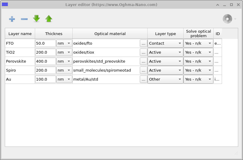
perovskites/std_perovskite) /
Spiro (200 nm) / Au (100 nm).
Set the perovskite as an Active layer so optical/electrical generation is calculated in it.
Perovskite solar cells are built as a stack of thin layers—some collect or transport charge, others absorb light. In OghmaNano the stack is edited with the Layer editor, accessible from the main window under the Device structure tab (see ??). The editor itself is shown in ??.
Each row in the editor corresponds to a layer with editable fields: Layer name, Thickness, Optical material, and Layer type (e.g. Active, Contact, Other). In this tutorial the active absorber is std_perovskite (a literature-averaged MAPbI₃ dataset).
Thickness is a key design parameter. Very thin absorbers (~50 nm) minimise transport distance but miss some light; thicker films (~400 nm) harvest more photons but increase the path that carriers must travel, raising the chance of recombination before collection. Performance therefore peaks at an intermediate thickness rather than increasing indefinitely—this trade-off is central to perovskite device design.
3. More about the Layer editor
The Layer editor is where you define the stack used by the simulator. Each row is a layer and each column controls how that layer behaves optically and electrically.
- Layer name – a human-readable label (e.g. FTO, TiO₂, Perovskite, Spiro, Au). The name does not affect the physics.
- Thickness – the physical thickness of the layer (units shown in the table, typically nm).
- Optical material – the n/k dataset used for optics (chosen from the databases). This is independent of the electrical model.
- Layer type – tells the solver how to treat the layer:
- Active: full drift–diffusion solved; carriers can be generated and recombine.
- Contact: an electrode where boundary conditions (work function, recombination velocity) are applied.
- Other: passive/transport layers; included in optics and electrostatics but without full generation–recombination physics.
4. Which layers should be active?
In principle, only layers that support both electrons and holes and where photogeneration or recombination occurs need to be marked as Active. In a minimal perovskite cell this would mean just the Perovskite absorber, while transport layers (e.g. TiO₂ and Spiro) would typically be left as passive layers. Contacts such as FTO and Au are never active, since they act only as electrodes.
However, in this tutorial the TiO₂ (electron transport layer) and Spiro (hole transport layer) have also been marked as Active. This setup allows you to investigate how carriers move through these transport layers, rather than treating them as idealised resistors. This distinction is important: it lets you capture transport-related losses in perovskites, whereas in OPV tutorials we normally keep transport layers as Other to simplify the physics.
As a general rule, only set extra layers as active when you are specifically interested in their transport properties or in phenomena like blocking contacts or S-shaped JV curves. Otherwise, keeping the number of active layers to a minimum will make simulations faster and results easier to interpret.