Many modern optoelectronic devices are fabricated over areas far larger than the microscopic scales typically simulated in semiconductor device physics. While the active layers of solar cells, OLEDs, and photodetectors may be only tens or hundreds of nanometres thick, the devices themselves can extend over centimetres or even metres. Simulating such structures using full three-dimensional drift–diffusion models quickly becomes computationally impractical.
In large-area devices the dominant limitations are often not vertical carrier transport through the active layer, but lateral current spreading, electrode resistance, and contact geometry. These effects determine how efficiently current can be collected from the device and frequently limit performance when scaling laboratory cells to practical device sizes.
To address this problem, OghmaNano includes a dedicated 3D circuit solver. Instead of solving the semiconductor transport equations everywhere in space, the solver converts the device geometry into a network of resistors and diodes that captures current flow across the full device area. This allows centimetre- and module-scale structures to be simulated efficiently while still reproducing the electrical behaviour of the underlying device physics.
The circuit solver is particularly useful for studying large-area solar cells, OLED panels, and photovoltaic modules. For example, the large-area contact tutorial demonstrates how electrode resistance affects current spreading, while the large-area PM6:Y6 solar cell tutorial shows how optical generation and diode elements can be incorporated into the circuit model. More complex device layouts, including interconnected cells, are explored in the perovskite module tutorial.
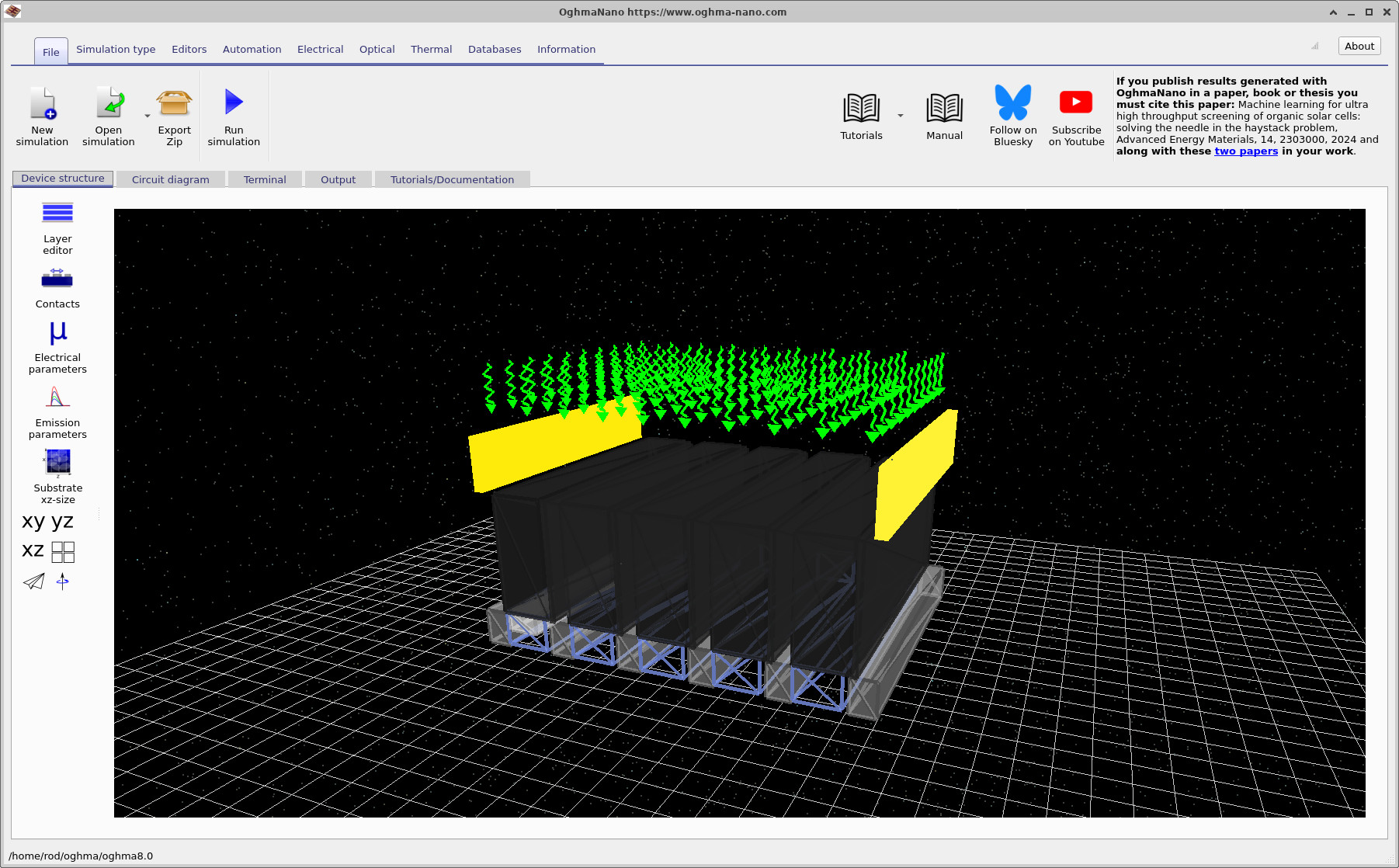
The circuit solver begins with the three-dimensional geometry of the device. Once the structure has been defined, the software generates a spatial mesh representing the physical layout. This mesh is then converted into an electrical network where each connection corresponds to a circuit element.
Conductive layers become resistive links, while active regions are represented by diode elements that reproduce the electrical behaviour of the device. The resulting network may contain thousands or millions of elements, but it can be solved efficiently using standard circuit-analysis techniques.
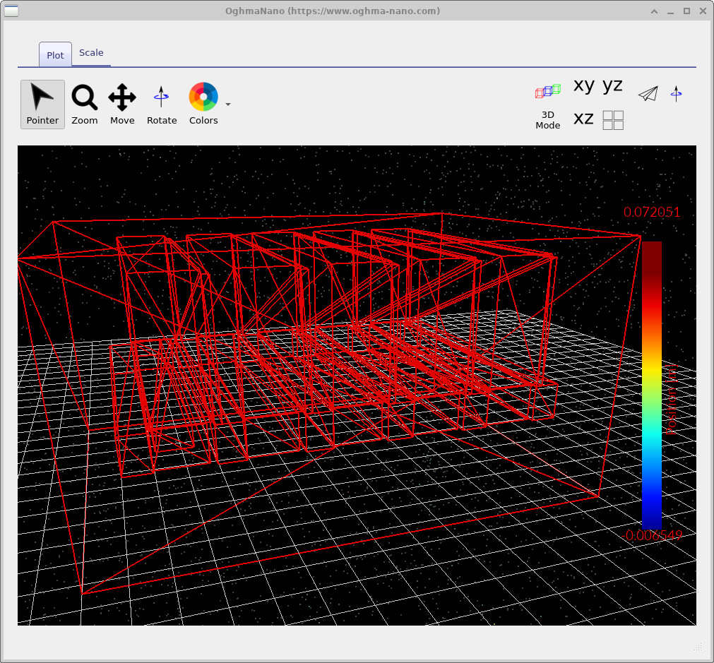
At every node in the network the solver enforces Kirchhoff’s current law:
$$ \sum_i I_i = 0 $$meaning that the total current flowing into each node must equal the total current flowing out. Solving these equations across the entire network determines how current distributes itself through the device geometry.
The circuit model uses several different types of electrical elements to represent the physical device:
The current through each diode element follows the standard diode equation
$$ I(V) = I_0 \left(e^{\frac{qV}{nkT}} - 1\right) - I_{ph} $$where \(I_0\) is the reverse saturation current, \(n\) is the ideality factor, and \(I_{ph}\) represents the photogenerated current supplied by the optical model.
Although the electrical behaviour is described using a circuit network, the optical properties of the device can still be simulated rigorously. OghmaNano includes several optical solvers including the transfer-matrix method.
These optical models calculate how light propagates and is absorbed throughout the device structure. The resulting spatial absorption profile is converted into a photogeneration term that feeds directly into the diode elements of the circuit network. In this way the solver combines accurate optical modelling with efficient large-area electrical simulation.
The 3D circuit solver is particularly useful for systems where the device area is much larger than the thickness of the active layers. Typical applications include:
In these devices the electrical behaviour is strongly influenced by electrode design and current spreading within conductive layers. By modelling these effects directly, the circuit solver allows researchers to explore different contact geometries and predict how device performance will scale with size.
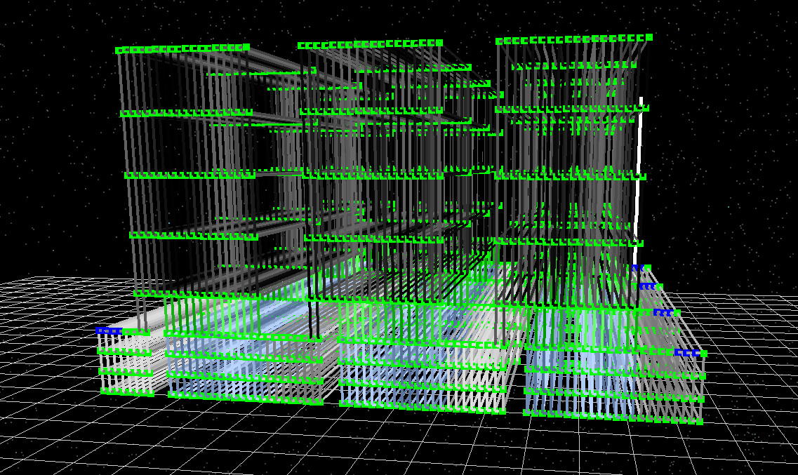
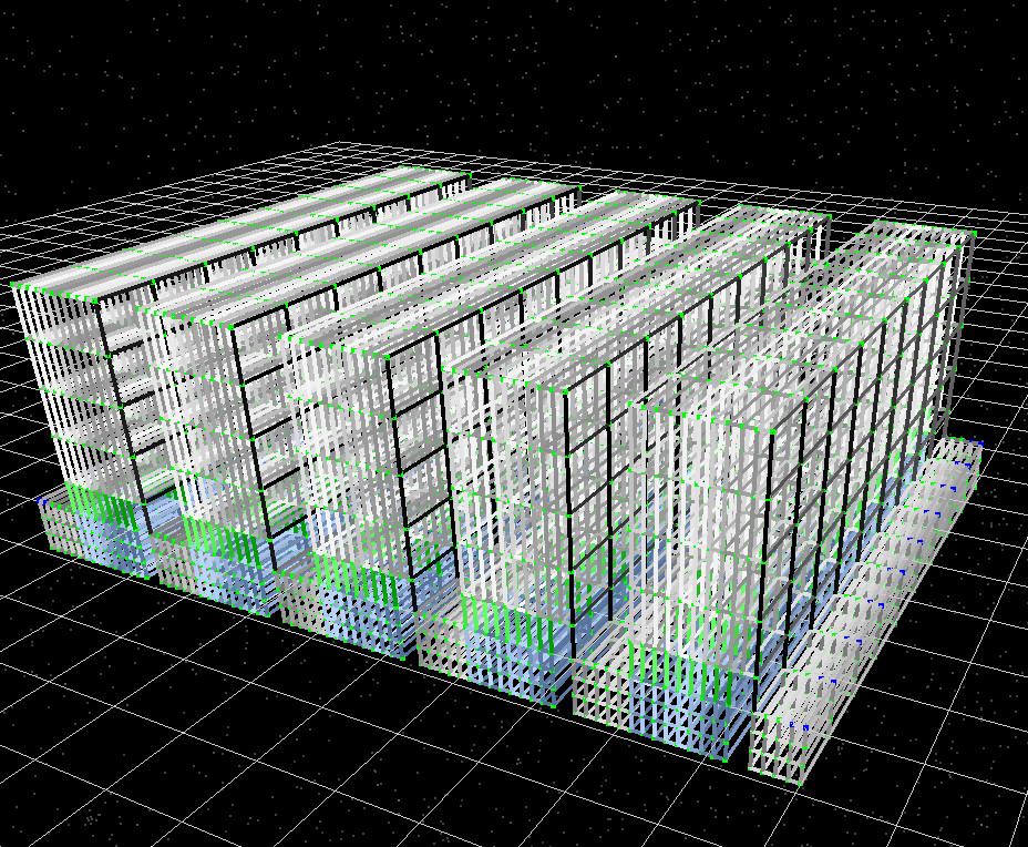
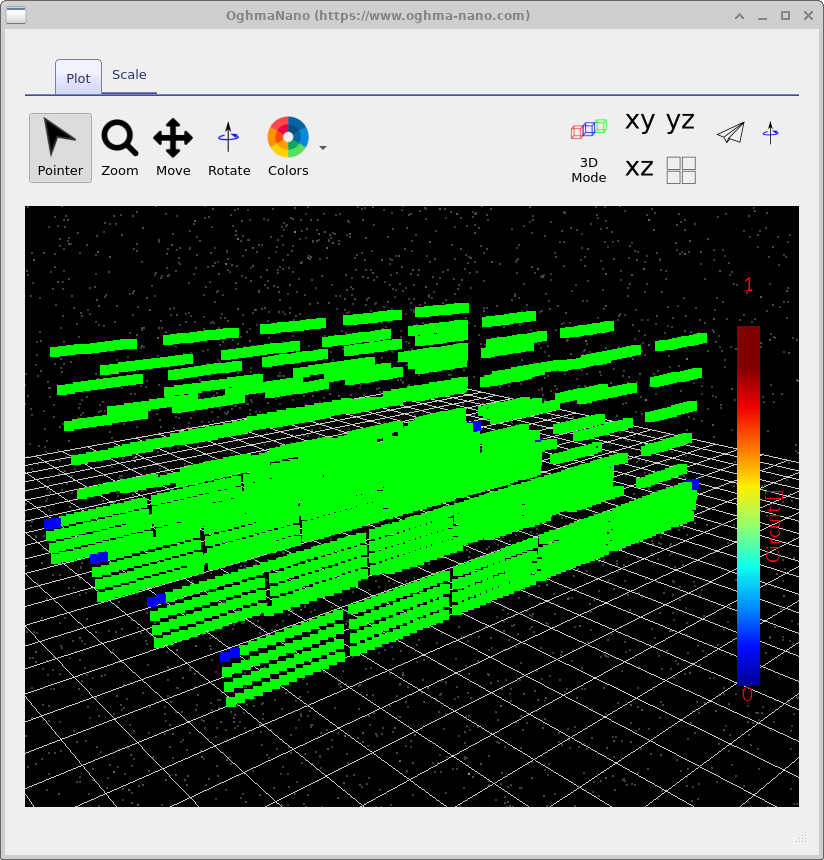
After the device geometry has been defined, OghmaNano automatically generates a three-dimensional circuit mesh from the structure. This mesh forms the foundation of the electrical model and defines how the physical geometry is converted into circuit elements.
An example of such a mesh is shown in Figure ??. Each connection in the mesh becomes a resistor or diode element depending on the material and layer from which it originates.
The solver also identifies extraction nodes, shown in Figure ??. These nodes represent the electrical contacts where current enters or leaves the device. Their distribution strongly influences how current spreads laterally through the circuit network.
OghmaNano includes several tutorials demonstrating how to use the 3D circuit solver for realistic device simulations. These examples guide users through the entire workflow, from defining the device geometry to analysing the resulting current–voltage characteristics.
A good starting point is the large-area contact simulation tutorial, which introduces current spreading and electrode resistance. From there you can move on to the large-area PM6:Y6 solar cell tutorial, which incorporates diode elements and optical generation.
For more advanced simulations, the perovskite module tutorial demonstrates how multiple devices can be interconnected to simulate full photovoltaic modules.
Try a large-area simulation.
Start with the large-area contact tutorial, then explore the PM6:Y6 solar cell example and the perovskite module tutorial.