OghmaNano contains an advanced transfer-matrix method (TMM) solver for modelling coherent thin-film optics in layered devices. The method is designed for problems in thin-film solar cells, OLED microcavities, optical filters, antireflection coatings, mirrors, and general planar multilayer stacks. Because the optical field is treated as a coherent wave propagating through a one-dimensional layered medium, the solver naturally captures reflection, transmission, interference, standing-wave formation, cavity enhancement, and wavelength-dependent absorption within one unified framework.
The same TMM framework can be applied to a wide range of layered optical structures, including multilayer optical filters, OLED device simulations with coherent thin-film optics, perovskite solar cells with optical generation, and organic photovoltaic devices. In smooth planar devices, the transfer-matrix approach is often the most direct way to understand how optical energy is redistributed across the stack and how that redistribution affects device performance.
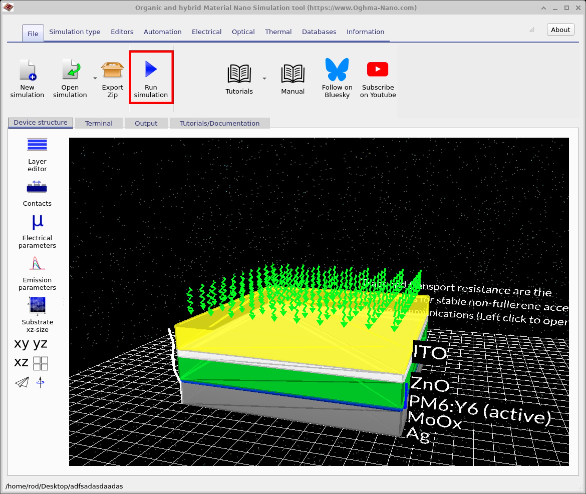
The user can define a layered structure, assign wavelength-dependent optical materials, calculate reflected and transmitted spectra, and inspect photon-density, absorption, and generation maps throughout the device. In more advanced simulations, the same optical engine can be coupled directly to OghmaNano’s electrical solvers, allowing optical absorption to generate photocurrent in solar cells or allowing electrically generated recombination profiles to feed an OLED outcoupling model.
In the transfer-matrix method, each thin film is represented by a matrix that relates the forward- and backward-propagating optical waves at its two interfaces. For a layer of refractive index \(n\), thickness \(d\), and phase thickness
\[ \delta = \frac{2\pi}{\lambda} n d, \]
a simple layer matrix may be written as
\[ M = \begin{bmatrix} \cos(\delta) & \dfrac{i}{n}\sin(\delta) \\ i n \sin(\delta) & \cos(\delta) \end{bmatrix}. \]
For a multilayer structure, the overall response is obtained by multiplying the matrices of the individual layers:
\[ M_{\mathrm{total}} = \prod_{j=1}^{N} M_j. \]
Once the total matrix is known, the complex reflection and transmission amplitudes can be extracted, and the measurable reflectance and transmittance follow from
\[ R = |r|^2, \qquad T = \frac{n_s}{n_0}|t|^2, \]
where \(n_0\) and \(n_s\) are the refractive indices of the incident medium and substrate. This one-dimensional wave treatment is computationally efficient, but it remains rigorous for planar coherent films and is therefore extremely well suited to multilayer optoelectronic devices.
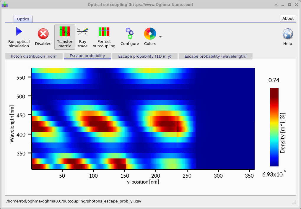
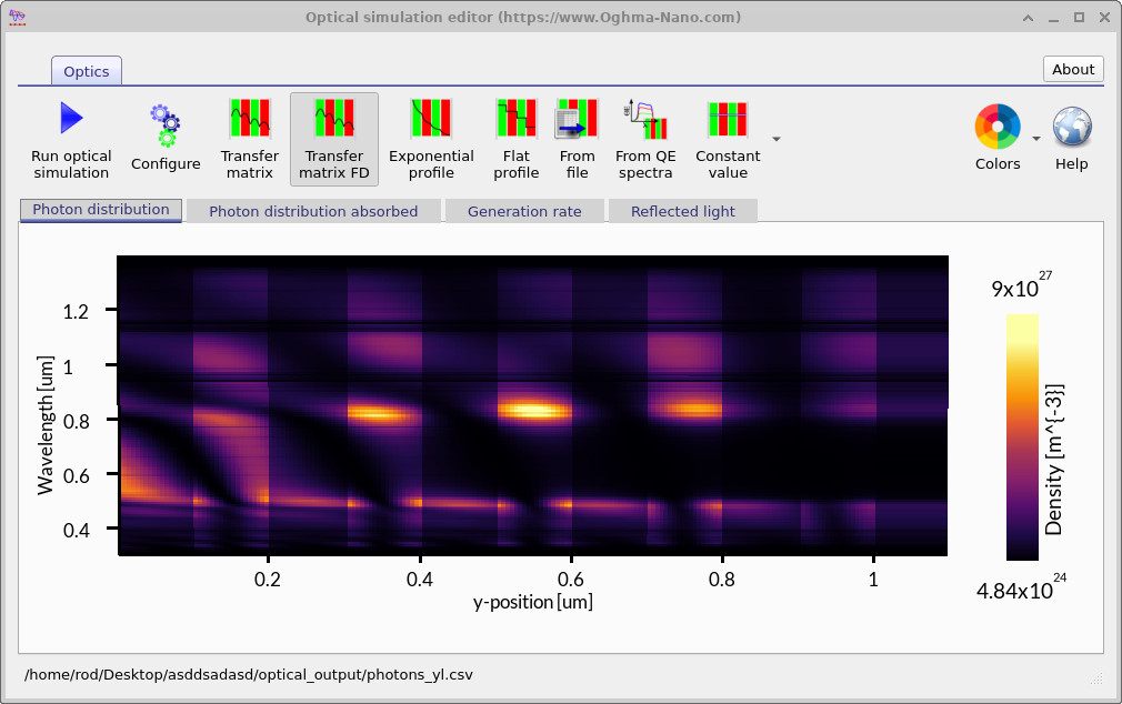
A major strength of TMM is that it resolves not only how much light is reflected or transmitted, but also where the optical field resides inside the device. The photon-density map shown in Figure ?? illustrates this directly: standing-wave patterns appear naturally inside the layered structure as a result of interference between forward- and backward-propagating waves.
This is crucial for solar-cell modelling, because absorption is not spatially uniform. The optical field can be enhanced or suppressed at different depths depending on wavelength, and this directly changes where electron–hole pairs are generated. In OghmaNano, the transfer-matrix solver can therefore provide a spatially resolved optical generation profile to the electrical solver, making it possible to model thin-film solar cells with realistic interference effects rather than uniform Beer–Lambert generation.
The same internal-field viewpoint is equally important for emissive devices. In OLEDs, light is not only generated within the stack, but is also redistributed by the optical cavity before escaping from the device. That is why coherent optics plays such a central role in OLED design.
In smooth planar OLEDs, the device acts as a thin-film optical cavity. Light generated at different positions inside the stack does not escape with equal probability at all wavelengths. Instead, the cavity modifies the spectral and angular outcoupling of the emission, and this can change strongly with layer thickness and emission-zone position.
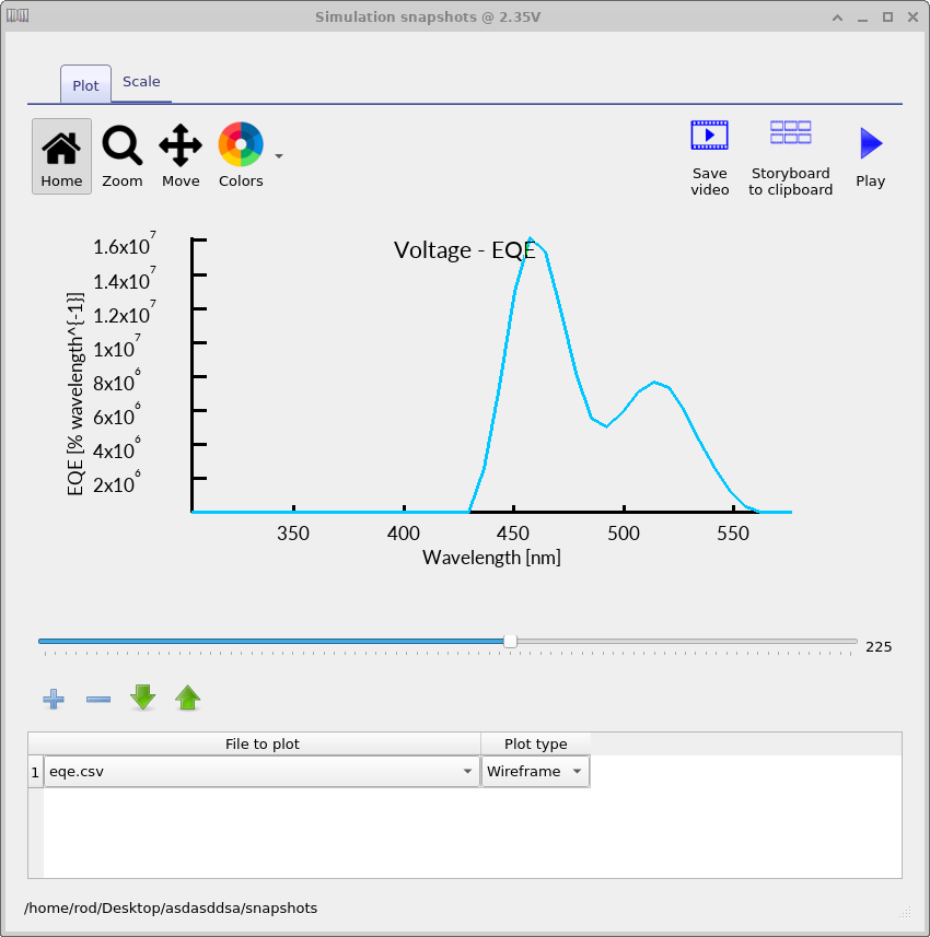
The escape-probability map shown in Figure ?? shows this clearly: some combinations of wavelength and depth couple efficiently out of the device, while others are suppressed. When the electrical recombination profile shifts with applied voltage, the effective emitted spectrum can shift with it. This is why the transfer-matrix engine is so useful in OLED modelling: it provides a direct route from recombination profile to emission spectrum, EQE spectrum, and colour coordinates.
The wavelength-dependent EQE spectrum in Figure ?? and the chromaticity trajectory in Figure ?? are examples of exactly this coupled electro–optical workflow. In OghmaNano, the TMM solver is therefore not just a passive optics post-processor: it is part of the full OLED device model.
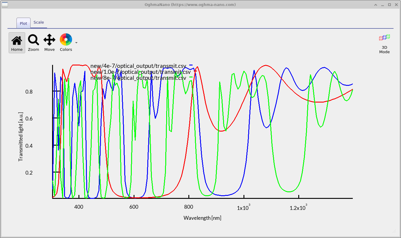
The transfer-matrix method is also a natural tool for designing multilayer optical filters. By changing layer thicknesses and refractive indices, the user can shift passbands, stopbands, and resonance features directly. This makes the method ideal for antireflection coatings, Bragg reflectors, cavity mirrors, and general spectral filters.
The scan result shown in Figure ?? illustrates how strongly the transmitted spectrum can change when the stack is modified. Because TMM is computationally inexpensive compared with full field solvers, it is particularly well suited to parameter scans and optimisation studies over thickness, wavelength range, or material choice.
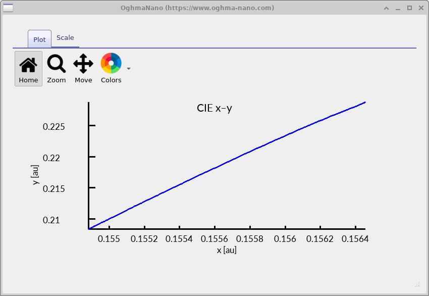
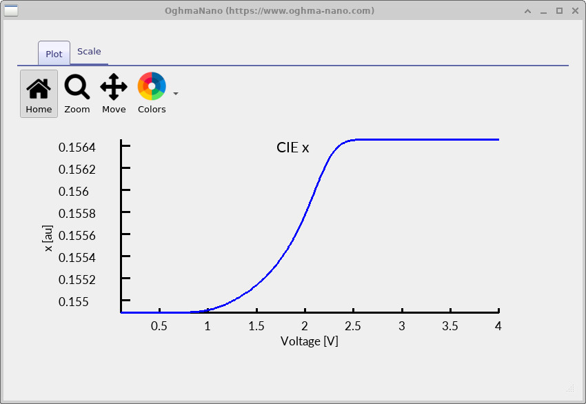
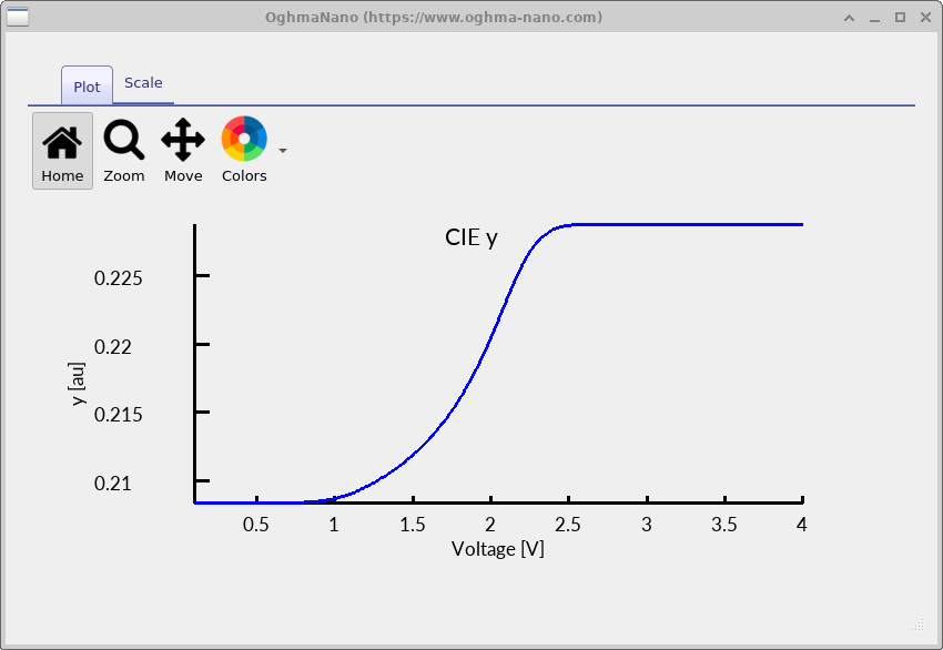
In addition to standard reflectance and transmittance spectra, OghmaNano’s TMM workflow can produce more device-specific optical outputs. For OLEDs this includes voltage-dependent EQE spectra and colour coordinates. For example, the calculated CIE \(x\), \(y\), and \(x\)-\(y\) trajectories shown in Figure ??, Figure ??, and Figure ?? make it possible to quantify colour drift as a function of operating point.
This is important in real device design. For solar cells, the key concern is where absorbed photons are converted into charge. For OLEDs, the key concern is often how cavity-modified emission changes brightness, spectrum, and perceived colour. The same transfer-matrix engine supports both use-cases.
The transfer-matrix method can be used for a broad range of one-dimensional wave-optics problems. In thin-film optics it is ideal for antireflection coatings, Bragg mirrors, optical filters, and cavity structures. In optoelectronics it is used for OLED outcoupling, thin-film solar-cell optical generation, perovskite stacks, and layered photodetectors. Wherever the device is well approximated by a planar stack and coherence across the layers matters, TMM provides a powerful and efficient solution.
Because the method is computationally light compared with full field solvers, it is especially useful for scanning layer thicknesses, testing candidate materials, and understanding design trends quickly. It therefore serves both as a practical design tool and as a way to build physical intuition about thin-film interference in layered devices.
OghmaNano includes several tutorials demonstrating how to use the transfer-matrix method in practical device problems. These examples take the user from basic multilayer optics to coupled electro–optical simulations.
Useful starting points include the optical filter tutorial, the OLED coherent thin-film optics tutorial, the perovskite optical absorption tutorial, and organic solar-cell tutorials. Taken together, these examples show how the same solver can be used for reflection and transmission analysis, cavity-modified emission, optical generation, EQE spectra, and colour prediction.
Try a transfer-matrix example.
Start with the optical filter tutorial for a quick introduction to multilayer interference, then move on to thin-film solar-cell optics or OLED coherent thin-film optics.
These examples show how to define a layered stack, calculate internal photon distributions, and connect coherent optics directly to device performance.