OghmaNano contains a 1D, 2D, and 3D drift–diffusion device solver that simultaneously solves the transport equations for both electrons and holes together with the electrostatic potential. The same physical framework can be applied to a wide range of semiconductor devices, including silicon PN junction diodes, silicon solar cells, gallium arsenide diodes, perovskite solar cells, and organic photovoltaic devices. In addition to the standard drift–diffusion framework, the model can resolve discretised trap-state populations at every mesh point. This makes it particularly well suited to disordered semiconductors, such as organic devices and perovskites, where transport and recombination are strongly influenced by localized states distributed in energy.
The solver therefore treats carrier transport not only in position space but also through the occupation of energetic trap states, allowing the internal electronic structure of a device to evolve dynamically under illumination or applied bias. This enables realistic simulation of trap-limited transport, recombination pathways, and transient behaviour that are difficult to capture using simplified lifetime-based models. Example applications include organic transistors, OLED devices, space-charge limited current devices, MOS capacitors, and 3D semiconductor junction simulations. Because the solver supports multidimensional transport and energy-resolved trap populations, it can be used for both simple layered devices and complex structures such as bulk-heterojunction morphologies or large-area solar cell modules.
Internally, the solver architecture is highly flexible and can be configured through a lightweight Lua scripting interface. This scripting layer allows the numerical solution strategy to be adapted without modifying the core solver itself. For example, different iteration schedules, operator splitting approaches, or staged solution procedures can be implemented to efficiently handle large or complex simulations. In practice this makes it possible to tailor how the coupled electrostatic and carrier-transport equations are solved, for example by solving subsets of the system sequentially or by applying directional sweeps across multidimensional meshes. The underlying physical equations remain unchanged, but the numerical strategy can be adapted to the size and structure of the problem being studied. For most simulations the default solver configuration is sufficient, but the scripting interface provides an additional level of control when needed. This allows the same drift–diffusion framework to be applied across a wide range of problems, from simple one-dimensional device stacks to large multidimensional simulations with complex geometries and trap-mediated transport.
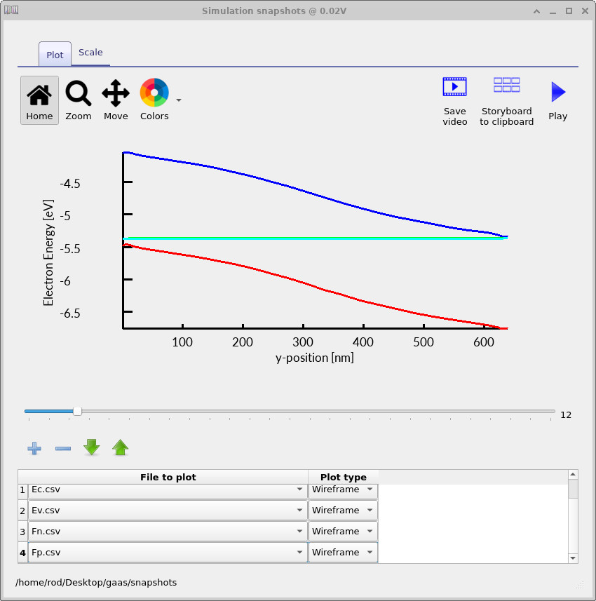
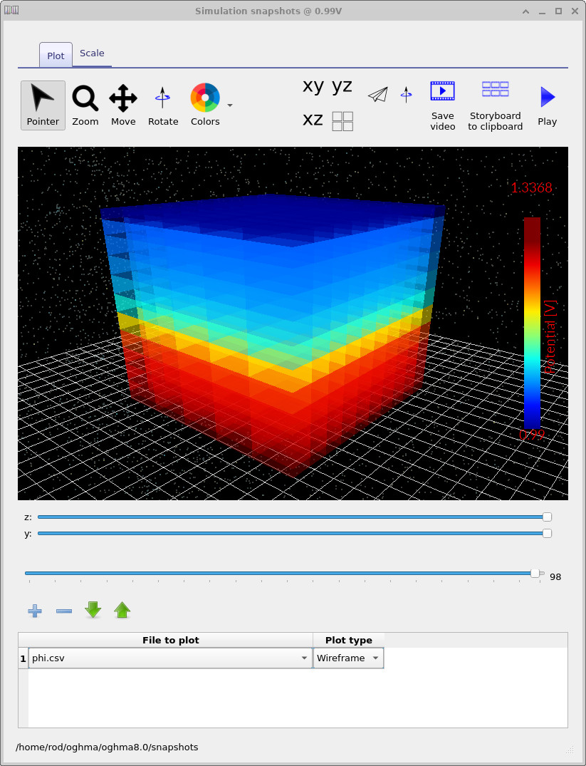
OghmaNano solves the coupled drift–diffusion and Poisson equations to describe charge transport in semiconductor devices. This provides the core electrical model used for simulating diodes, solar cells, photodiodes, and other layered or multidimensional structures under steady-state and transient conditions.
For electrons, the current density is written as
$$\mathbf{J_n}=q \mu_e n_f \nabla E_c + q D_n \nabla n_f$$and for holes
$$\mathbf{J_p}=q \mu_h p_f \nabla E_v - q D_p \nabla p_f$$Carrier conservation is enforced through the continuity equations
$$\nabla \mathbf{J_n}=q(R-G+\frac{\partial n}{\partial t})$$ $$\nabla \mathbf{J_p}=-q(R-G+\frac{\partial p}{\partial t})$$These equations are solved self-consistently with Poisson’s equation to determine the internal electrostatic potential, carrier densities, band bending, and current flow throughout the device.
In ordered or weakly disordered materials, recombination can often be represented using a free-to-free recombination model. In OghmaNano this is written as
$$R_{free}=k_{r}(n_{f}p_{f}-n_{0}p_{0})$$where \(k_r\) is the free-carrier recombination coefficient, and \(n_f\) and \(p_f\) are the free electron and hole densities. This form is useful when recombination occurs directly between mobile carriers without requiring explicit trap-state dynamics.
For materials or operating conditions where three-particle recombination becomes important, Auger recombination can also be included:
$$R^{AU}=(C^{AU}_{n}n+C^{AU}_{p}p)(np-n_{0}p_{0})$$where \(C^{AU}_{n}\) and \(C^{AU}_{p}\) are the Auger coefficients for electrons and holes. This is particularly relevant for high carrier densities, heavily doped materials, or device regions with strong carrier accumulation.
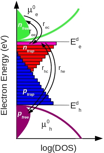
For disordered semiconductors, such as organic semiconductors, amorphous materials, and other trap-rich systems, simple free-to-free recombination is often not sufficient. In these materials, charge transport and recombination are strongly influenced by localized states distributed in energy. OghmaNano therefore includes an explicit treatment of Shockley-Read-Hall trapping, de-trapping, and recombination, allowing trap populations to evolve dynamically during the simulation.
In the representation shown in Figure 2, the free electron and hole populations are labelled \(n_{free}\) and \(p_{free}\), while trapped carriers occupying localized states are denoted \(n_{trap}\) and \(p_{trap}\). The model resolves carrier capture and emission processes between these populations, making it possible to simulate non-equilibrium trap occupation and time-dependent trapping effects.
For a single trap level the population balance is given by
$$\frac{\partial n_t}{\partial t}=r_{ec}-r_{ee}-r_{hc}+r_{he}$$where the four transition rates describe capture and escape processes between free carriers and trap states. This treatment is especially important for modelling disordered materials because it allows the solver to represent slow trapping, delayed release, carrier-density-dependent transport, and recombination pathways that cannot be captured using a simple lifetime approximation.
Table 1: SRH capture and escape rates. |
The carrier escape probabilities are
$$e_n=v_{th}\sigma_{n} N_{c} \exp \left ( \frac{E_t-E_c}{kT}\right )$$ $$e_p=v_{th}\sigma_{p} N_{v} \exp \left ( \frac{E_v-E_t}{kT}\right )$$where \(v_{th}\) is the thermal velocity of the carriers, \(\sigma_{n,p}\) are the capture cross sections, and \(N_c\), \(N_v\) are the effective density of states for electrons and holes.
Trap distributions are defined through a density-of-states function
$$\rho^{e/h}(E)=N^{e/h}\exp(E/E_{u}^{e/h})$$where \(E_u\) is the characteristic slope energy describing the energetic disorder of the material.
The density of trap states for a discrete level is calculated by averaging the density of states over the trap energy interval \(\Delta E\)
$$N_{t}(E)=\frac{\int^{E+\Delta E/2}_{E-\Delta E/2} \rho^{e}(E)dE}{\Delta E}$$Each trap level maintains its own quasi-Fermi level, allowing the solver to capture non-equilibrium trap occupation during transient simulations. This energy-resolved SRH framework is one of the main features that makes OghmaNano particularly well suited to disordered-material device physics.
In addition to bulk transport, OghmaNano includes models for carrier transport across material interfaces and heterojunctions. While carriers normally cross interfaces through the same drift–diffusion processes that govern bulk transport, real devices often contain energetic barriers that strongly suppress current flow. To capture these effects the solver can apply additional interface transport models that represent processes such as tunnelling or trap-assisted transfer.
For example, direct tunnelling across a thin barrier can be represented using a simplified form
$$ \boldsymbol{J} = A(n-n^{eq})V\exp(-B\sqrt{\phi}) $$where \( \phi \) is the barrier height extracted from the band structure and \(A\) and \(B\) are phenomenological constants describing the interface transmission probability.
A detailed description of these models and their implementation is provided in the interface theory section of the manual.
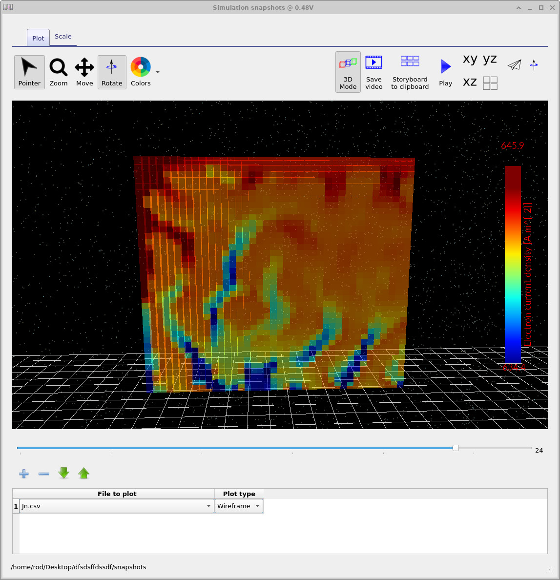
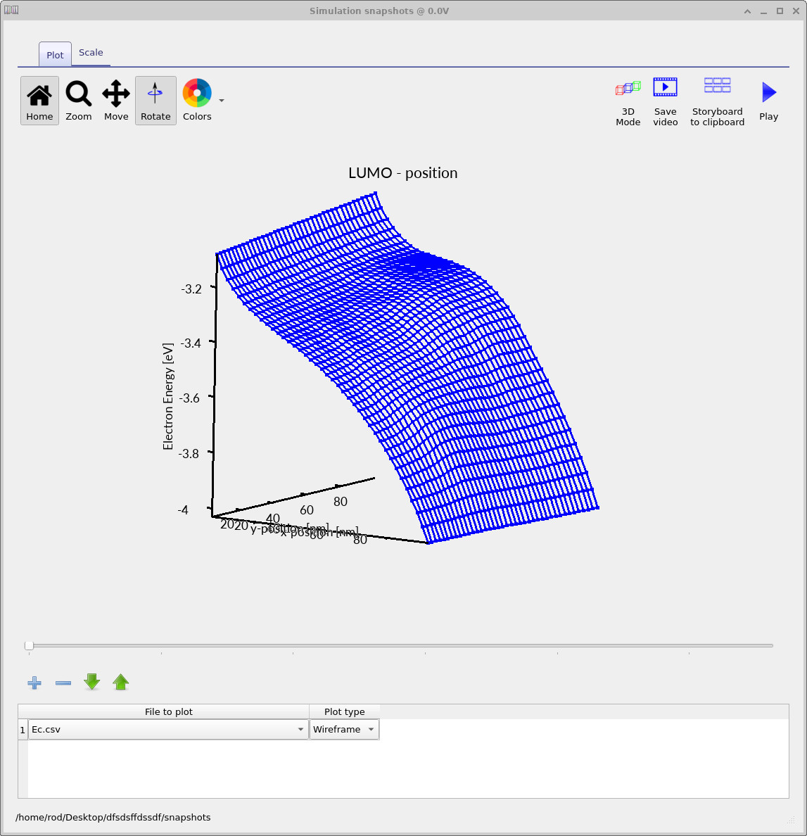
The same drift–diffusion framework can be applied to a wide range of real device classes. At the simplest level, it can be used to model silicon solar cells and large-area photovoltaic structures, where carrier generation, recombination, built-in fields, and contact losses determine the final current-voltage characteristics, as illustrated by Figure ??.
The solver is equally applicable to compound-semiconductor junctions, including gallium arsenide diodes, where transport, band offsets, and recombination can be studied under forward or reverse bias. More generally, the same equations can be used for photodetectors, emissive diodes, and related semiconductor structures in which charge injection, extraction, and recombination are central to device operation, as represented in Figure ??.
Because OghmaNano also supports multidimensional transport and structured geometries, the model can be extended beyond simple planar stacks to more complex device layouts and microfabricated structures, as suggested by Figure ??. In practice this means the same solver can be used for perovskite solar cells, organic devices, semiconductor photodiodes, and a broad range of junction-based optoelectronic systems without changing modelling framework.

Explore the full physics stack.
See the core physics modules in the manual for detailed descriptions.