

How are band structures calculated in perovskites? Eight-band k·p theory
Why Calculate the Electronic Band Structure?
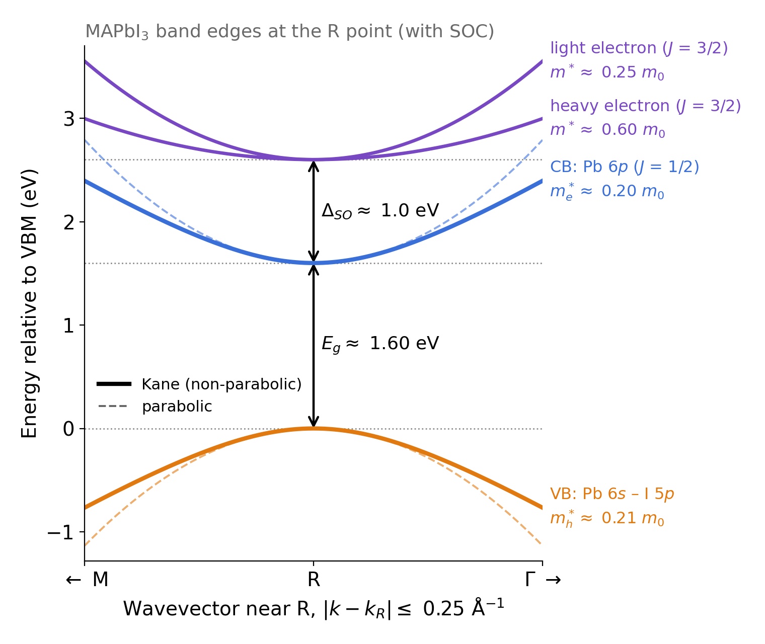
Calculating the electronic band structure of a perovskite means determining which electron energies are allowed at different wavevectors within its crystal. The resulting energy bands provide information about the band gap, effective masses, carrier velocities and the electronic states available to electrons and holes. An example calculated for MAPbI3 is shown in ??.
Why is this useful? Once the electronic band structure and corresponding wavefunctions have been calculated, they provide the starting point for predicting a wide range of semiconductor properties. These include acoustic phonon scattering, polar optical phonon (Fröhlich) scattering, carrier relaxation times, electron and hole mobilities, carrier concentrations, density of states, optical absorption, spontaneous emission, stimulated emission and optical gain. The electronic structure can also be used to investigate how these properties change with temperature, carrier density and material composition. In this way, calculating the band structure is often the first step towards understanding both the electrical and optical behaviour of a semiconductor.
Here we explain how OghmaNano calculates the band structures of three-dimensional CsPbX3 and MAPbX3 perovskites (X = Cl, Br or I), starting with Schrödinger's equation and progressing to the eight-band k·p model. The mathematical formulation and material parameterisation follow Gawarecki et al., “Eight-band k·p description and material gain for selected cubic and pseudo-cubic perovskites”, Physical Review Applied 22, 014058 (2024): published paper (DOI) | freely accessible arXiv preprint. The explanations and illustrations on this page describe the numerical workflow independently; the original publication contains the complete matrix formulation and derivation.
For instructions on running a simulation, choosing a material or exploring mixed-halide compositions, see the practical perovskite band structure and mobility tutorial. A more detailed explanation of how electronic states interact with polar optical phonons is available on our Fröhlich scattering theory page.
Starting with Schrödinger's Equation
To understand how electronic bands form in a semiconductor, consider an electron moving through a crystal. Rather than experiencing the potential of a single isolated atom, the electron encounters a repeating arrangement of atoms, each contributing to the overall crystal potential. This is illustrated in ??, where the potential of an isolated atom is compared with the periodic potential of a crystal.
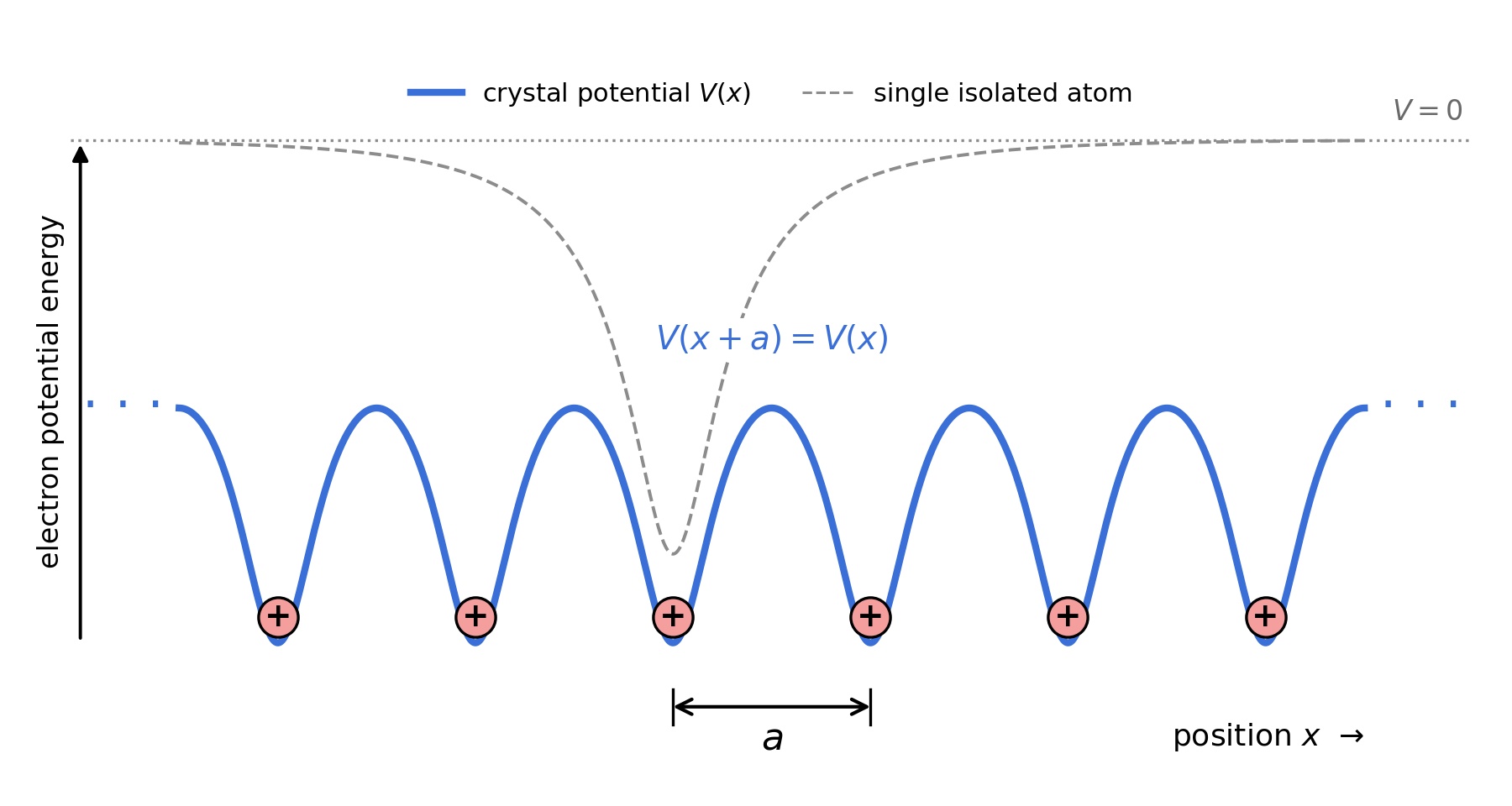
The important feature is that the crystal potential repeats at regular intervals, determined by the lattice spacing \(a\). Mathematically, this means that \(V(x+a)=V(x)\). An electron moving through such a periodic potential can occupy a range of allowed energy states, which collectively form the electronic bands of the material.
To calculate these states, we start with the time-independent Schrödinger equation:
\[ \hat H\psi(\mathbf r)=E\psi(\mathbf r). \]
Here, \(\psi\) is the electron wavefunction, \(E\) is its energy, and \(\hat H\) is the Hamiltonian: the mathematical operator describing the energy of the electron. In a simple one-electron description of the crystal, the Hamiltonian contains two contributions: the kinetic energy of the electron and the potential energy associated with the atomic lattice:
\[ \hat H_0 = -\frac{\hbar^2}{2m_0}\nabla^2 + V_{\mathrm{crystal}}(\mathbf r). \]
The first term describes the electron's kinetic energy, while \(V_{\mathrm{crystal}}(\mathbf r)\) represents the periodic potential shown in ??. Solving Schrödinger's equation for this potential gives the allowed electron energies and corresponding wavefunctions, from which the electronic band structure can be constructed.
In principle, the electronic structure can be calculated by resolving the full atomic potential, for example using density functional theory (DFT). However, if we are primarily interested in the electronic states close to the band gap, it is often more efficient to describe a smaller number of important states using an effective Hamiltonian.
This is the idea behind the k·p method. We retain Schrödinger's eigenvalue equation but replace the simple one-electron Hamiltonian with a matrix describing several interacting electronic bands. For metal halide perovskites, OghmaNano uses the eight-band formulation developed by Gawarecki et al., which includes the strong spin–orbit coupling characteristic of these materials. The numerical parameters of this Hamiltonian were obtained by fitting the model to first-principles DFT band structures (Gawarecki et al., Sections III–IV).
Why Calculate Around the R Point?
To calculate the electronic band structure, we need to consider how the electron energy changes with its wavevector (or crystal momentum). Just as we describe positions in real space using \(x\), \(y\) and \(z\), we describe positions in momentum space using \(k_x\), \(k_y\) and \(k_z\). The repeating structure of a crystal gives rise to a corresponding region in momentum space called the Brillouin zone.
We are particularly interested in the region where the valence and conduction bands are closest together, since this determines the semiconductor's band gap. In familiar semiconductors such as GaAs, the fundamental direct band gap occurs at the centre of the Brillouin zone, known as the \(\Gamma\) point. For the cubic lead halide perovskites considered here, however, the direct band gap occurs at a corner of the Brillouin zone, known as the R point (Gawarecki et al., Fig. 1).
Rather than calculating the electronic structure across the entire Brillouin zone, we therefore start at the R point and examine how the energies change as we move a small distance away from it. We describe this displacement using the wavevector \(\mathbf{k}\):
\[ \mathbf{K}=\mathbf{K}_R+\mathbf{k}, \qquad \mathbf{k}=(k_x,k_y,k_z). \]
Here, \(\mathbf{K}_R\) is the position of the R point, while \(\mathbf{k}\) describes how far we have moved away from it. Consequently, \(\mathbf{k}=0\) in our calculation corresponds to the R point, not the centre of the Brillouin zone.
For each new value of \(\mathbf{k}\), we construct and solve the eight-band Hamiltonian, obtaining a new set of allowed electron energies. Repeating this calculation as we move away from R produces the electronic band structure shown earlier in this page.
One further feature of these perovskites is worth noting: unlike GaAs, where the valence-band edge is predominantly p-like and the conduction-band edge is s-like, the ordering is reversed. The valence band is predominantly s-like, while the nearby conduction bands are p-like. This difference is taken into account when constructing the eight-band Hamiltonian (Gawarecki et al., Fig. 1).
3. The eight electronic states included in the model
The model keeps eight nearby electronic states, counting spin. Its basis is built from an s-like valence orbital \(|S\rangle\) and three p-like conduction orbitals \(|X\rangle\), \(|Y\rangle\) and \(|Z\rangle\), each combined with spin-up or spin-down. The strong spin–orbit interaction mixes the p-like orbitals and spin into states labelled by total angular momentum \(|j,m_j\rangle\). The resulting states fall into three groups:
| Group (cubic notation) | Number of states | What they describe |
|---|---|---|
| \(\Gamma_{6v}^{+}\) | 2 | s-like valence-band pair, \(j=1/2\) |
| \(\Gamma_{6c}^{-}\) | 2 | Lowest, spin–orbit split-off conduction-band pair, \(j=1/2\) |
| \(\Gamma_{8c}^{-}\) | 4 | Higher heavy- and light-electron conduction states, \(j=3/2\) |
In a compact notation, the eight functions in the basis are
\[ \begin{aligned} &|S,\uparrow\rangle,\quad |S,\downarrow\rangle,\\ &|\tfrac32,\tfrac32\rangle_c,\quad |\tfrac32,\tfrac12\rangle_c,\quad |\tfrac32,-\tfrac12\rangle_c,\quad |\tfrac32,-\tfrac32\rangle_c,\\ &|\tfrac12,\tfrac12\rangle_c,\quad |\tfrac12,-\tfrac12\rangle_c. \end{aligned} \]
For example, the valence pair is simply \(|S\rangle\otimes|\uparrow\rangle\) and \(|S\rangle\otimes|\downarrow\rangle\). The six conduction states are particular combinations of \(X,Y,Z\) and spin. The full coefficients, phases and exact ordered basis are given in Appendix A of Gawarecki et al.; those conventions matter when constructing the individual matrix entries. In pseudo-cubic MAPbX3, reduced symmetry can further split the four-state upper conduction group (their Section IV).
4. Constructing the perovskite Hamiltonian
We now replace the single-band energy operator with an \(8\times8\) Hermitian matrix acting on the eight states. Grouping the basis into its upper conduction, lower conduction and valence sectors gives the block form introduced in Eq. (1) of Gawarecki et al.:
\[ H(\mathbf k)= \begin{pmatrix} H_{8c,8c} & H_{8c,6c} & H_{8c,6v}\\ H_{6c,8c} & H_{6c,6c} & H_{6c,6v}\\ H_{6v,8c} & H_{6v,6c} & H_{6v,6v} \end{pmatrix}. \]
The diagonal blocks describe how each band group changes with wavevector. The off-diagonal blocks describe the coupling between groups; this coupling is important because it changes the curvature and character of the resulting bands. The opposite off-diagonal entries are related by Hermitian conjugation: \(H_{b,a}=H_{a,b}^{\dagger}\).
To see the main energy scales without reproducing the full appendix matrix, consider the R point itself. With the top of the valence band taken as the energy reference, the basic band-edge structure is
\[ E_v(0)=0,\qquad E_{6c}(0)=E_g,\qquad E_{8c,\pm}(0)=E_g+\Delta_c\pm\frac{\delta}{3}. \]
Thus, \(E_g\) places the lowest conduction band, \(\Delta_c\) places the upper conduction group, and \(\delta\) allows an additional upper-band separation when the symmetry is reduced. In the cubic CsPbX3 limit, \(\delta=\zeta=0\) and \(P_{\parallel}=P_z\); the pseudo-cubic MAPbX3 materials can have non-zero values of these symmetry-dependent parameters.
Two particularly simple diagonal blocks show how the reference energies and quadratic dispersion are introduced (\(I_2\) is the two-state identity matrix and \(k^2=k_x^2+k_y^2+k_z^2\)):
\[ \begin{aligned} H_{6c,6c} &= \left(E_g+\frac{\hbar^2}{2m_0}\gamma'_1 k^2\right)I_2,\\ H_{6v,6v} &= \frac{\hbar^2 k^2}{2m_0}I_2. \end{aligned} \]
As one example of an off-diagonal coupling, the lower conduction and valence pairs are connected by
\[ H_{6c,6v}=-\frac{1}{\sqrt{3}}\left[ P_{\parallel}(\sigma_x k_x+\sigma_y k_y) +\sigma_z(P_z k_z-i\zeta)\right], \]
where \(\sigma_x,\sigma_y,\sigma_z\) are the familiar two-state Pauli spin matrices. This displays the important distinction between direction-dependent coupling and the extra pseudo-cubic term. These illustrative blocks follow Section IV of Gawarecki et al.; their full upper conduction block and its couplings contain additional angular-momentum matrices and the \(\gamma'_2,\gamma'_3,\delta\) terms.
The entries also contain linear and quadratic wavevector terms. For instance, the in-plane and out-of-plane coupling strengths enter through combinations proportional to \(P_{\parallel}k_x\), \(P_{\parallel}k_y\) and \(P_zk_z\). Terms proportional to \(\gamma'_1 k^2\), \(\gamma'_2\) and \(\gamma'_3\) influence curvature and direction dependence. The explicit invariant blocks are supplied in Section IV, and the ordered matrix with its auxiliary definitions is supplied in Appendix A of the original paper.
In practice, OghmaNano assembles the complete numerical matrix using the selected material parameters and the current values of \(k_x,k_y,k_z\). It is this matrix, rather than the simple free-electron Hamiltonian, whose eigenvalues are calculated at each wavevector.
5. Sweeping momentum to obtain the electronic bands
Once we have a Hamiltonian, calculating a band structure becomes a repeated eigenvalue problem. Choose a wavevector displacement from R, construct \(H(\mathbf k)\), and solve
\[ H(\mathbf k)\,\mathbf u_n(\mathbf k) =E_n(\mathbf k)\,\mathbf u_n(\mathbf k),\qquad n=1,\ldots,8. \]
The eight real eigenvalues \(E_n\) are the eight band energies at that wavevector. Each corresponding eigenvector \(\mathbf u_n\) tells us how the eight basis states mix to form that electronic state. We repeat the operation across a sequence of wavevectors. As a simple example, a sweep along the local x direction uses
\[ \mathbf k_0=(0,0,0),\quad \mathbf k_1=(\Delta k,0,0),\quad \mathbf k_2=(2\Delta k,0,0),\quad \ldots \]
\[ H(\mathbf k_i)\longrightarrow \{E_1(\mathbf k_i),\ldots,E_8(\mathbf k_i)\} \quad\text{for each }i. \]
Plotting those energies against wavevector gives the familiar E–k diagram. To follow a different crystal direction, the path is changed accordingly; for example, a local diagonal path varies more than one component of \(\mathbf k\). A three-dimensional mesh samples \(k_x,k_y,k_z\) together. Band indices may be tracked using neighbouring eigenvector overlaps when bands approach or cross, instead of relying on energy ordering alone.
\(E_g,\Delta_c,P,\gamma'\ldots\)
\((k_x,k_y,k_z)\)
8 × 8 matrix
8 eigenvalues + states
band structure
The resulting band gap and band curvature are immediately useful. Near a simple parabolic extremum, the directional effective mass can be related to the second derivative of energy:
\[ \frac{1}{m_i^*}=\frac{1}{\hbar^2} \frac{\partial^2E}{\partial k_i^2}, \]
with the usual positive hole-mass convention applied to the valence-band maximum. The full bands, rather than only a constant effective mass, can then be used in subsequent carrier statistics and transport calculations.
6. Material parameters and where they enter the model
The published values below are taken from Table I of Gawarecki et al.. The authors fitted the eight-band description to hybrid-functional DFT results including spin–orbit coupling (see their Sections III–IV). These are the numerical inputs for the six pure materials supplied in the OghmaNano perovskite library.
| Parameter | CsPbCl3 | CsPbBr3 | CsPbI3 | MAPbCl3 | MAPbBr3 | MAPbI3 |
|---|---|---|---|---|---|---|
| aexp (Å) | 5.605 | 5.886 | 6.294 | 5.675 | 5.901 | 6.329 |
| aDFT (Å) | 5.654 | 5.914 | 6.293 | 5.735 | 5.985 | 6.355 |
| Eg (eV) | 2.744 | 2.073 | 1.416 | 3.007 | 2.277 | 1.549 |
| Δc (eV) | 1.444 | 1.476 | 1.494 | 1.506 | 1.508 | 1.500 |
| δ (eV) | 0 | 0 | 0 | 0.045 | 0.057 | 0.075 |
| ζ (eV) | 0 | 0 | 0 | 0.016 | 0.030 | 0.045 |
| P∥ (eV·Å) | 9.233 | 8.948 | 8.601 | 8.878 | 8.623 | 8.097 |
| Pz (eV·Å) | 9.233 | 8.948 | 8.601 | 9.896 | 9.302 | 9.058 |
| γ′1 | 1.643 | 2.183 | 2.997 | 1.581 | 2.144 | 2.967 |
| γ′2 | 0.190 | 0.394 | 0.683 | 0.140 | 0.190 | 0.286 |
| γ′3 | −0.691 | −1.081 | −1.169 | −0.599 | −1.060 | −1.150 |
| mv (m0) | 0.189 | 0.158 | 0.125 | 0.210 | 0.178 | 0.141 |
| γ1 | 3.424 | 4.157 | 5.221 | 3.228 | 3.954 | 5.001 |
| γ2 | 1.081 | 1.381 | 1.795 | 0.963 | 1.094 | 1.302 |
| γ3 | 0.199 | −0.094 | −0.057 | 0.225 | −0.155 | −0.134 |
The role of the parameters is summarised below:
- \(E_g\): fundamental gap between the valence-band maximum and the lowest conduction state; sets the \(6c\) band-edge energy.
- \(\Delta_c\): principal spin–orbit separation between the lower and upper conduction groups; shifts the \(8c\) block relative to \(6c\).
- \(\delta\) and \(\zeta\): extra symmetry-dependent splitting and coupling in the pseudo-cubic description. Both vanish for the cubic CsPbX3 parameter sets.
- \(P_{\parallel}\) and \(P_z\): coupling between s-like valence and p-like conduction states, in the in-plane and vertical directions. Their units here are eV·Å.
- \(\gamma'_1,\gamma'_2,\gamma'_3\): coefficients of the wavevector-squared terms; they affect the average band curvature, anisotropy and band mixing, including contributions from states beyond this eight-state model.
- \(a_{\mathrm{exp}}\), \(a_{\mathrm{DFT}}\): lattice constants provided for structural context. They are not interchangeable fitting coefficients of the displayed Hamiltonian.
- \(m_v\) and unprimed \(\gamma_1,\gamma_2,\gamma_3\): derived quantities included in the source paper for comparison; use the primed parameters in the matrix to avoid counting the explicitly included band coupling twice (see Eqs. (2)–(4) in the paper).
The pure-material files contain the tabulated values. Mixed-halide material scripts interpolate between the endpoint parameters before building the matrix, so the same calculation can be performed for a user-selected composition. The practical setup is described in the mixed-halide tutorial.
7. From the calculated bands to carrier mobility
Solving the eight-band problem provides more than a plot of energy against wavevector. The eigenvalues describe the available electronic energies; the eigenvectors describe the corresponding electronic states. Combined with Fermi–Dirac occupation, the bands can be used to calculate carrier populations and locate the Fermi level at a selected carrier density.
To obtain mobility, we must also determine how frequently carriers lose momentum while moving through the crystal. A major intrinsic interaction in polar metal halide perovskites is Fröhlich scattering: an electron or hole interacts with the electric field generated by a longitudinal optical (LO) phonon, absorbing or emitting phonon energy \(\hbar\omega_{LO}\).
\[ E_f=E_i\pm\hbar\omega_{LO},\qquad \mathbf k_f=\mathbf k_i\pm\mathbf q. \]
The allowed transitions depend on the band energies, electronic states, phonon energy and dielectric properties of the material. Their scattering rates are converted into momentum relaxation times and combined with the band transport properties to estimate the Fröhlich-limited mobility. In the simplest parabolic-band picture, this connection is expressed as
\[ \mu\simeq\frac{e\tau_{\mathrm{tr}}}{m^*}. \]
The full explanation of LO phonon absorption, emission, Fröhlich coupling and the scattering-rate calculation is given in the separate Fröhlich Scattering: LO Phonons and Carrier Mobility theory page. For screenshots showing how to run the perovskite calculation, inspect its band structure and plot electron and hole mobilities, return to the step-by-step OghmaNano tutorial.
References and further reading
Primary model: K. Gawarecki, M. Wiśniewski, M. Polak, R. Kudrawiec and M. Gładysiewicz, “Eight-band k·p description and material gain for selected cubic and pseudo-cubic perovskites”, Physical Review Applied 22, 014058 (2024). DOI: 10.1103/PhysRevApplied.22.014058; arXiv:2306.08643 (free preprint). See especially Section IV and Appendix A for the full Hamiltonian, and Table I for the parameters.