

GaN/AlGaN Quantum Well: 8-Band Wurtzite k·p Tutorial
1. Introduction
In this tutorial we will calculate the electronic states and optical response of a GaN quantum well between two AlGaN barriers using OghmaNano's eight-band wurtzite k·p model. The example has a 10 nm GaN well and two 20 nm AlGaN layers. We will first run the supplied example, then inspect the conduction- and valence-subband dispersions and the resulting optical spectra.
The distinction between wurtzite and zincblende matters here. Both are semiconductor crystal structures, but wurtzite has a preferred hexagonal c-axis. The different crystal symmetry changes the valence-band splitting, the coupling between electronic states and the strength of light polarized in different directions. Consequently, a zincblende eight-band calculation cannot simply be reused with GaN material parameters.
2. Opening the eight-band wurtzite example
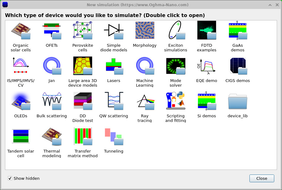
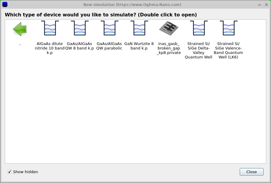
From the File ribbon, click New simulation. In the window that appears, double-click GaAs demos (??). Despite the category name, it also contains the nitride and silicon quantum-well examples. Double-click GaN Wurtzite 8 band k.p in the next window (??). This opens the prepared material stack and selects the appropriate demonstration.
3. Inspecting the GaN/AlGaN quantum well
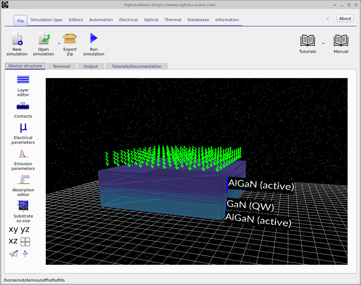
The main window shows the three-layer structure (??). In the actual quantum-well calculation, confinement is along the thickness of this stack: the electronic envelope functions vary across the layers, while the dispersion plots describe motion parallel to them.
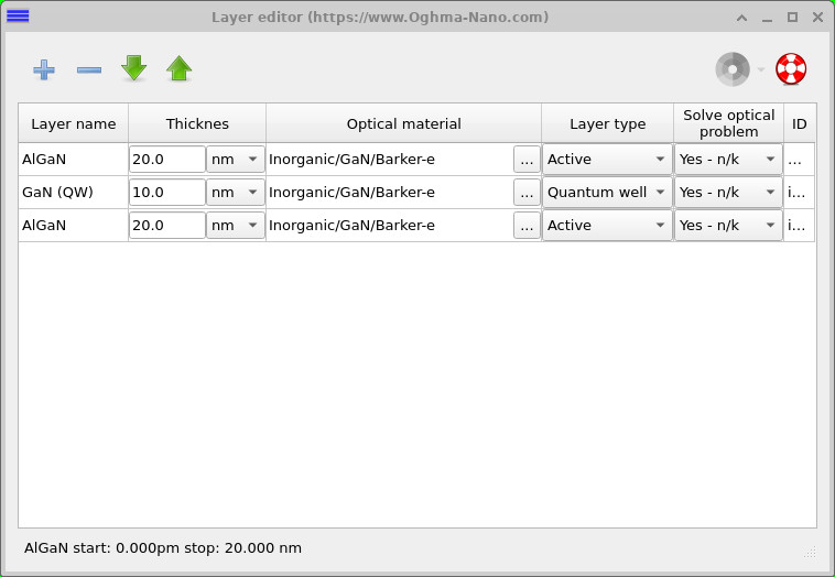
Click Layer editor in the left toolbar. As shown in ??, the example uses the following geometry:
| Layer | Thickness | Type |
|---|---|---|
| AlGaN | 20 nm | Active / barrier |
| GaN (QW) | 10 nm | Quantum well |
| AlGaN | 20 nm | Active / barrier |
Leave the supplied material settings unchanged for your first run. The screenshot establishes the layer thicknesses, but does not show the Al mole fraction, strain configuration or polarization parameters; these should be checked in the example's material settings before using it to represent a particular experimental wafer.
4. Why use an eight-band wurtzite Hamiltonian?
A simple parabolic model assigns an effective mass to each carrier and assumes that its energy changes approximately as the square of its in-plane wavevector. This is useful near a band extremum, but it cannot describe how the various valence states mix with one another as the wavevector increases. In wurtzite materials, the hexagonal crystal environment also distinguishes motion and light polarization along the c-axis from those in the perpendicular plane.
The eight-band approach retains a conduction-like orbital and three valence-like orbitals, each with two spin components. Conceptually, an eigenstate has the form
\[ \Psi_{n,\mathbf{k}_{\parallel}}(\mathbf{r})= e^{i\mathbf{k}_{\parallel}\cdot\mathbf{r}_{\parallel}} \sum_{\alpha=1}^{8}F_{n\alpha}(z)u_{\alpha}(\mathbf{r}), \]
where the functions \(F_{n\alpha}(z)\) describe confinement across the well, and \(u_\alpha\) are the eight Bloch basis states. A given confined state can therefore have contributions from more than one valence-band orbital; this is why describing every coloured curve using a single fixed heavy-hole or light-hole label can be misleading away from the band edge.
The wurtzite valence-band ordering is affected by crystal-field and spin–orbit interactions. In a compact notation, the calculation solves
\[ H_{8\times8}\!\left(k_x,k_y,-i\frac{\partial}{\partial z}\right) \mathbf{F}_n(z)=E_n(\mathbf{k}_{\parallel})\,\mathbf{F}_n(z). \]
Notice that the in-plane wavevector is retained explicitly, whereas the growth-direction wavevector is replaced by a differential operator. Repeating this eigenvalue problem for different \(k_{\parallel}\) produces the subband-dispersion plots below. A fuller discussion of the basis, crystal-field terms and material coefficients is given in the wurtzite k·p theory chapter.
5. Run the simulation
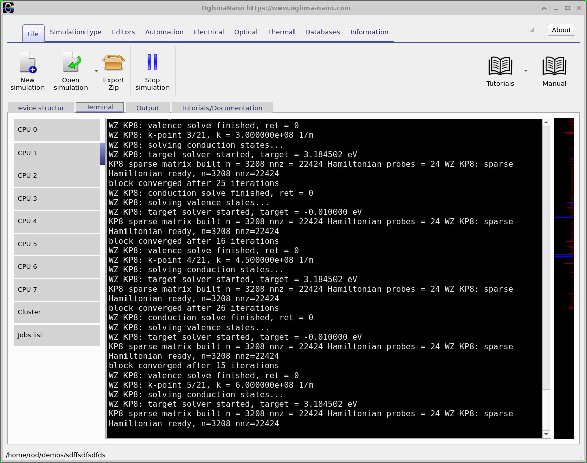
Return to the File ribbon and press Run simulation. Open the Terminal tab to follow progress. In ??, the terminal identifies the WZ KP8 solver, reports sparse-matrix assembly, prints convergence information, and advances through the sampled wavevectors. It solves the electron and valence states separately at each point.
Because this is a multicomponent envelope-function problem, it is more involved than solving an independent scalar parabolic well for each band. Wait until the eigensolver and subsequent optical calculations have finished before inspecting the resulting files.
5.1 Inspecting the optical transition strengths
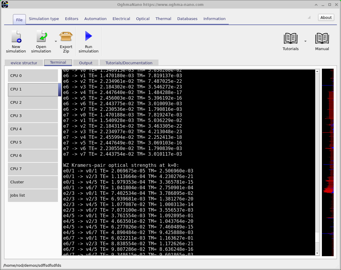
Later in the run, the terminal reports the optical matrix-element strengths (??). For a conventional c-plane wurtzite structure, TE refers to the optical electric field perpendicular to the c-axis, while TM refers to its component parallel to that axis. These polarizations need not couple equally strongly to a given electronic transition.
A useful way to think about the optical strength is the squared transition matrix element:
\[ M_{cv}^{(\mathbf{e})}(\mathbf{k}_{\parallel})= \left\langle\Psi_{c,\mathbf{k}_{\parallel}}\middle| \mathbf{e}\!\cdot\!\mathbf{p}\middle| \Psi_{v,\mathbf{k}_{\parallel}}\right\rangle, \qquad S_{cv}^{(\mathbf{e})}\propto\left|M_{cv}^{(\mathbf{e})}\right|^2. \]
Here \(\mathbf{e}\) specifies the light polarization and \(\mathbf{p}\) is the momentum operator. A state can be present in the electronic band structure yet contribute very little to a particular optical polarization if its matrix element is small. The relative TE/TM values in the terminal therefore provide additional physical information beyond the positions of the energy levels alone.
6. Understanding the calculated electronic bands
The horizontal axis of each band plot is the in-plane wavevector \(k_{\parallel}\), not position within the quantum well. The vertical axis is the energy of a confined subband. At \(k_{\parallel}=0\), each curve begins at one of the discrete confinement energies. Moving to the right shows how the same electronic state disperses when the carrier moves parallel to the layers.
6.1 Conduction-band states
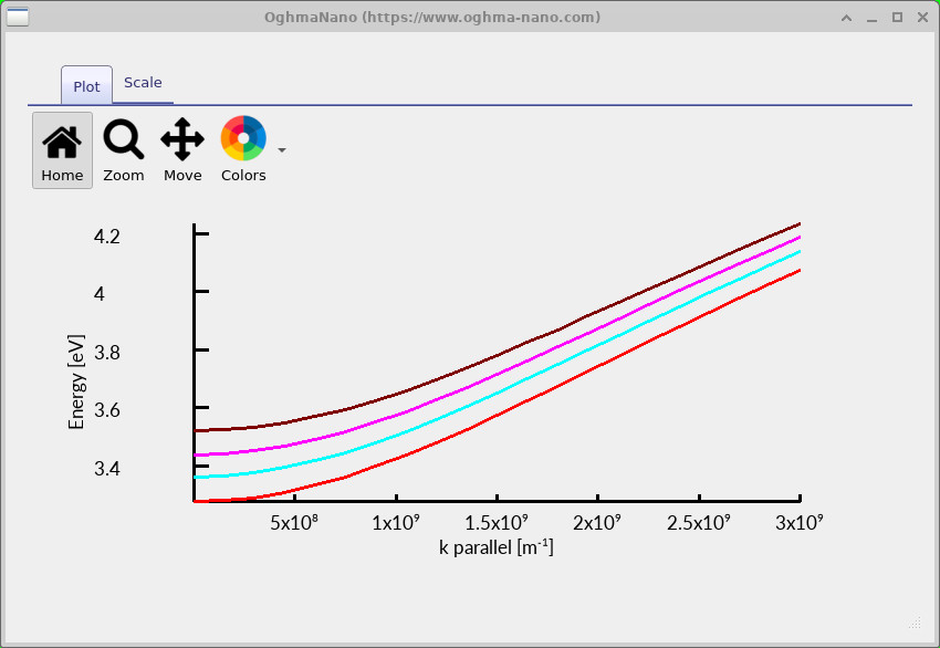
Open the conduction-band output and inspect the dispersion in ??. Several confined levels are visible, beginning at different energies close to the GaN band edge. At small wavevector, a useful approximation for a conduction subband is
\[ E_{c,n}(k_{\parallel})\simeq E_{c,n}(0) +\frac{\hbar^2 k_{\parallel}^2}{2m_{e,\parallel}^{*}}. \]
The term \(E_{c,n}(0)\) contains the confinement energy, while \(m_{e,\parallel}^{*}\) describes the carrier's response to in-plane motion. This relation helps explain the approximately rising curves, although the full eight-band calculation retains interband coupling rather than imposing a fixed parabolic shape.
6.2 Valence-band states
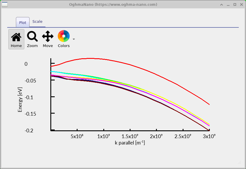
The valence-band plot (??) is more complicated. Its upper branch initially rises away from \(k_{\parallel}=0\) before bending down; several lower branches have visibly different curvatures. Such shapes are possible in a coupled wurtzite valence-band model, in which crystal-field splitting, spin–orbit coupling, confinement and band mixing act together.
This plot should not be interpreted as evidence that every coloured curve has a fixed A-, B- or C-band identity throughout the entire wavevector range. To make a definitive assignment, inspect the contributions of the underlying eigenvector components. Similarly, unusual off-centre extrema are worth comparing against the chosen material and strain parameters if using the model quantitatively.
7. Optical transitions, stimulated emission and absorption
The electronic bands determine the energies of possible optical transitions, but transition strengths also depend on the electron and hole wavefunctions, polarization, and carrier occupations. At a common in-plane wavevector, the photon energy for a vertical transition is
\[ \hbar\omega=E_{c,n}(\mathbf{k}_{\parallel}) -E_{v,m}(\mathbf{k}_{\parallel}). \]
Fermi's golden rule explains why the optical matrix elements printed in the terminal matter. In schematic form, the rate for a transition is
\[ W_{v\rightarrow c}^{(\mathbf{e})}= \frac{2\pi}{\hbar}\left|H_{cv}^{\prime(\mathbf{e})}\right|^2 \delta\!\left(E_c-E_v-\hbar\omega\right). \]
The perturbation matrix element \(H'_{cv}\) depends on light polarization and the participating states. The delta function imposes energy conservation; when constructing a practical spectrum, the contributions of the allowed transitions are summed over the sampled states and broadened. The carrier occupation factors then determine whether absorption or stimulated emission dominates at a particular wavelength. A convenient schematic net factor is \(f_c-f_v\), where \(f_c\) and \(f_v\) are the electron occupations of the conduction and valence states respectively.
Because the GaN well has a wide electronic gap, its calculated spectra appear in the near-ultraviolet, predominantly around 330–370 nm in the supplied example. The wavelength and photon energy are related by \(E_{\gamma}=hc/\lambda\).
7.1 Stimulated emission and net gain
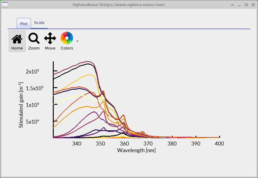
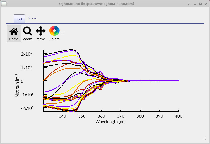
The stimulated-emission plot (??) contains a family of spectra for different carrier conditions. The net-gain calculation (??) accounts for the competition between emission and absorption. A positive material gain indicates amplification within this electronic model, but it does not by itself demonstrate that a complete laser cavity has reached threshold: confinement factor and resonator losses must also be considered.
7.2 Absorption
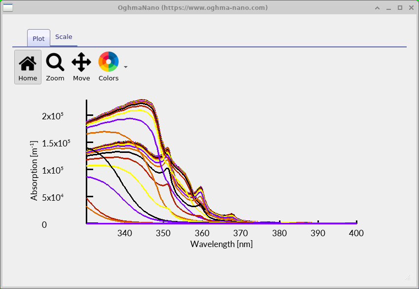
The absorption results are shown in ??. Their edges and spectral features are determined by the separations between occupied valence and available conduction states, weighted by their optical matrix elements. In a wurtzite well, the corresponding TE and TM spectra may differ because the orbital content of a state determines how strongly it couples to each polarization.
The features in these spectra are results of the configured model and broadening. They should not automatically be identified with particular excitonic peaks: a single-particle k·p interband calculation is not, by itself, a full treatment of electron–hole Coulomb-bound excitons.
8. Spontaneous emission
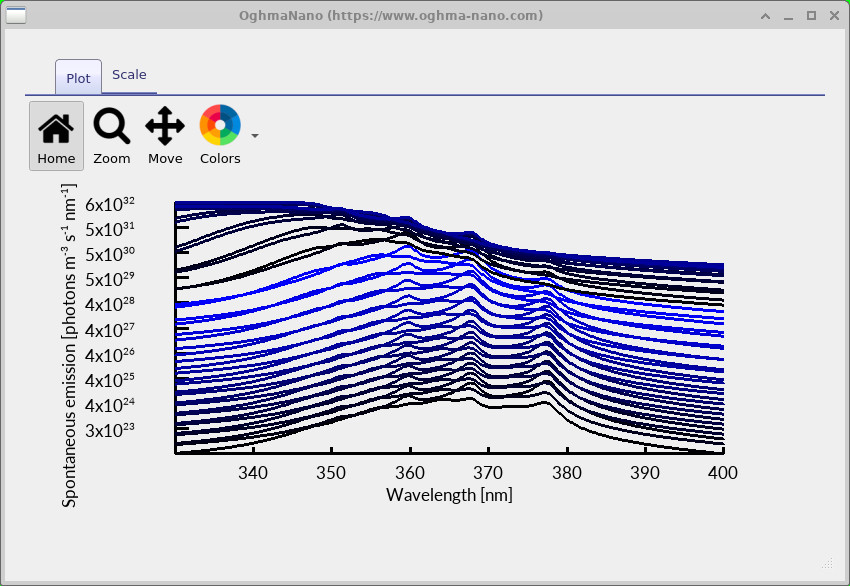
Unlike stimulated emission, spontaneous emission occurs without an incident photon initiating the transition. It depends on the availability of an electron in the conduction state and an empty state in the valence band (a hole). Its electronic occupation factor is therefore proportional to
\[ R_{\mathrm{sp}}(\omega)\ \propto\ \sum_{c,v,\mathbf{k}_{\parallel}} \left|M_{cv}(\mathbf{k}_{\parallel})\right|^2 f_c(1-f_v)\,L\!\left(E_c-E_v-\hbar\omega\right), \]
where \(L\) denotes the chosen spectral broadening and the proportionality leaves out photonic prefactors. The result is plotted in ??. The logarithmic scale makes it possible to compare spectra spanning many orders of magnitude. Notice the optical features near the shorter-wavelength part of the spectrum and the change in overall magnitude across the plotted conditions.
9. Try it yourself
💡 Two useful follow-up calculations:
- Change the GaN well width. Try reducing the central 10 nm layer to 7 nm, leaving the barriers unchanged. Recalculate the eigenstates and compare the lowest conduction levels and optical transition energies. Stronger confinement will generally increase the separation between confined levels, although the detailed valence response is multiband.
- Compare TE and TM strengths. Use the optical strengths reported by the terminal to identify transitions that strongly favour one polarization. Look at how this relates to the valence-state character, rather than assuming that all transitions contribute equally to the spectrum.
✅ What should you look for?
A narrower well usually pushes electron confinement energies upward and changes the hole levels, shifting the available interband transition energies. TE/TM ratios can vary markedly from one pair of states to another because they probe different orbital components of the wurtzite wavefunctions. For a quantitative material study, also examine the effects of alloy composition, strain and polarization fields.
📘 To learn more about the physical origin of these results, continue to the eight-band wurtzite k·p theory page, or compare against the zincblende eight-band tutorial.