What is the Transfer Matrix Method?
1. Introduction
The Transfer Matrix Method (TMM) is a fast and computationally efficient technique used to model electromagnetic wave propagation in multilayer thin-film optical structures. It is widely used in optics, photonics, and semiconductor device simulation to calculate wavelength-dependent reflection, transmission, absorption, interference, and electric field distributions in optical stacks composed of layered materials with different refractive indices. Applications include thin-film solar cells, OLED microcavities, dielectric mirrors, anti-reflection coatings, distributed Bragg reflectors (DBRs), optical filters, waveguide coatings, and other planar photonic devices.
TMM is derived directly from Maxwell’s equations and provides a simplified one-dimensional solution of the electromagnetic wave equation for stratified media. Instead of solving the full vector electromagnetic field throughout a multidimensional simulation domain, the method represents light inside each layer as forward and backward propagating waves travelling through a complex refractive index profile.
Because the Transfer Matrix Method reduces the optical problem to a sequence of compact matrix operations, it is extremely fast compared with full-wave numerical techniques such as FDTD. Despite its computational simplicity, TMM accurately captures coherent thin-film interference effects including standing-wave formation, Fabry–Perot resonances, optical cavity behaviour, and field enhancement inside dielectric stacks and multilayer optical coatings. This makes the method one of the most widely used approaches for modelling coherent optics in layered thin-film devices.
2. Physical principle of the Transfer Matrix Method
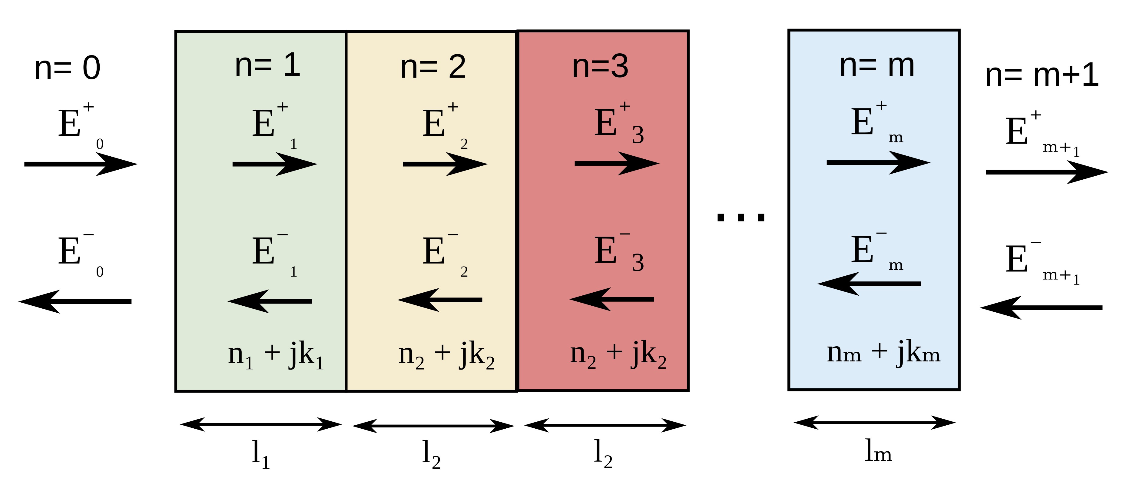
The Transfer Matrix Method represents the optical field inside each layer as the superposition of a forward and backward propagating electromagnetic wave:
\[ E(z)=E^{+}e^{-jkz}+E^{-}e^{jkz} \]
where \(E^{+}\) and \(E^{-}\) are the amplitudes of the forward and backward travelling waves respectively, \(z\) is the propagation direction through the multilayer structure, and
\[ k=\frac{2\pi \tilde{n}}{\lambda}, \qquad \tilde{n}=n+j\kappa \]
is the complex optical wavevector, where \(n\) is the refractive index, \(\kappa\) describes optical absorption, and \(\lambda\) is the wavelength in vacuum. As illustrated in ??, the forward and backward propagating waves are coupled at every material interface through partial reflection and transmission.
This wave representation is obtained from the solution of the one-dimensional Helmholtz wave equation derived from Maxwell’s equations in a homogeneous medium:
\[ \frac{d^2E(z)}{dz^2}+k^2E(z)=0 \]
At each interface, Maxwell’s electromagnetic boundary conditions are applied to ensure continuity of the tangential electric and magnetic fields. These conditions produce the Fresnel reflection and transmission coefficients:
\[ r=\frac{n_1-n_2}{n_1+n_2}, \qquad t=\frac{2n_1}{n_1+n_2} \]
where \(n_1\) and \(n_2\) are the complex refractive indices of the neighbouring layers. These coefficients determine how the forward and backward propagating waves are partially reflected and transmitted at every material interface.
3. Constructing the transfer matrix
As illustrated in ??, the optical field inside each layer is represented by a forward propagating wave \(E^+\) and a backward propagating wave \(E^-\):
\[ \mathbf{E}= \begin{bmatrix} E^{+} \\ E^{-} \end{bmatrix} \]
As the electromagnetic wave propagates through a layer of thickness \(d\), the optical field accumulates phase and attenuation. This propagation through the layer can be written as:
\[ \begin{bmatrix} E^{+}(d) \\ E^{-}(d) \end{bmatrix} = \begin{bmatrix} e^{-jkd} & 0 \\ 0 & e^{jkd} \end{bmatrix} \begin{bmatrix} E^{+}(0) \\ E^{-}(0) \end{bmatrix} \]
At the boundary between two materials, part of the optical field is transmitted and part is reflected. This interface relation can also be written in matrix form:
\[ \begin{bmatrix} E^{+}_2 \\ E^{-}_2 \end{bmatrix} = \frac{1}{t} \begin{bmatrix} 1 & r \\ r & 1 \end{bmatrix} \begin{bmatrix} E^{+}_1 \\ E^{-}_1 \end{bmatrix} \]
The complete multilayer optical structure is therefore represented as a sequence of propagation and interface matrices:
\[ \mathbf{E}_{out} = M_N I_N \cdots M_2 I_2 M_1 I_1 \mathbf{E}_{in} \]
where \(M\) represents propagation through a layer and \(I\) represents transmission and reflection at an interface. The optical response of the entire device can therefore be calculated using a sequence of simple matrix multiplications.
This approach allows reflection, transmission, absorption, interference, and standing-wave formation in complex multilayer optical structures to be calculated extremely efficiently while remaining directly connected to Maxwell’s equations. Because the Transfer Matrix Method solves the optical wave equation directly, it naturally captures thin-film interference effects. As light reflects from multiple interfaces, the reflected waves interfere constructively or destructively depending on the optical phase accumulated within each layer, \( \phi = \frac{2\pi n d}{\lambda} \), where \(n\) is the refractive index, \(d\) the layer thickness, and \(\lambda\) the wavelength. As a result, even nanometre-scale thickness changes can strongly modify the optical response of a device. This interference physics governs the operation of anti-reflection coatings, Fabry–Perot cavities, distributed Bragg reflectors (DBRs), optical filters, OLED microcavities, and thin-film solar cells.
4. What does the Transfer Matrix Method calculate?
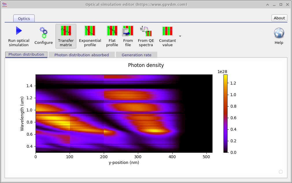
Once the global transfer matrix of the multilayer structure has been constructed, the electromagnetic field can be calculated at any position inside the device. This allows the spatial optical field distribution, reflection, transmission, and absorption to be determined throughout the structure.
Because the Transfer Matrix Method solves the optical wave equation directly, coherent interference effects naturally emerge from the simulation. As light reflects multiple times between interfaces, constructive and destructive interference produce standing-wave patterns inside the device.
The photon density distribution shown in ?? illustrates how the optical field intensity varies throughout a multilayer structure. Regions of high optical field intensity correspond to enhanced photon density caused by optical interference and cavity effects.
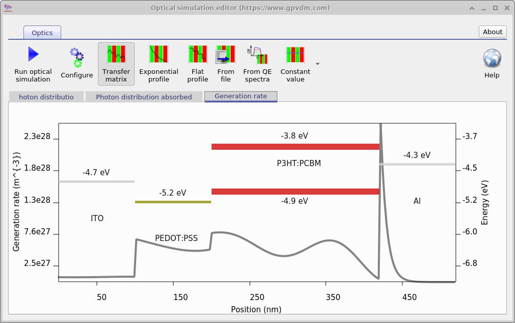
The local optical field distribution directly determines where photons are absorbed inside the device. By combining the electromagnetic field with the material absorption coefficient, the optical generation profile can be calculated:
\[ G(z)=\alpha(z)\Phi(z) \]
where \(G(z)\) is the local charge-generation rate, \(\alpha(z)\) is the optical absorption coefficient, and \(\Phi(z)\) is the local photon flux. An example generation profile calculated using the Transfer Matrix Method is shown in ??.
These calculations are widely used in thin-film solar cells, OLEDs, optical coatings, dielectric mirrors, optical sensors, and resonant microcavity devices. Because the Transfer Matrix Method is computationally inexpensive, complete optical spectra and internal field distributions can usually be calculated in a fraction of a second.
5. Advantages and limitations of the Transfer Matrix Method
The Transfer Matrix Method (TMM) is widely used because it combines strong physical accuracy with extremely low computational cost. For layered optical structures, TMM can reproduce the same thin-film interference physics as much larger full-wave simulations while requiring orders of magnitude less memory and computation time.
👉 Using TMM in practice: See the Transfer Matrix simulation tool to learn how TMM is implemented in OghmaNano.
Key advantages of TMM include:
- Very fast simulations: ideal for parameter sweeps and device optimisation.
- Accurate thin-film interference: rigorously captures coherent interference and standing-wave effects.
- Direct optical outputs: electric field, photon density, and absorption profiles are easily extracted.
- Excellent for planar multilayers: particularly useful for OLEDs, solar cells, optical coatings, and DBRs.
- Easy coupling to electrical models: optical generation profiles can be passed directly into drift–diffusion simulations.
However, TMM also has important limitations. The method fundamentally assumes that the optical structure can be treated as approximately one-dimensional, with material properties varying mainly along the growth direction. As a result, arbitrary three-dimensional scattering geometries are difficult to model rigorously.
- Primarily one-dimensional: limited to layered structures.
- Limited scattering physics: diffuse scattering and random roughness are not treated rigorously.
- No arbitrary geometries: gratings, nanoparticles, textured surfaces, and photonic crystals generally require full-wave solvers.
- Coherence assumptions: standard TMM assumes coherent propagation inside each layer.
For strongly three-dimensional optical problems, numerical methods such as FDTD, finite-element methods (FEM), or rigorous coupled-wave analysis (RCWA) are generally more appropriate. TMM is therefore best suited to planar multilayer devices where interference effects are important but the structure remains approximately one-dimensional.
8. Summary
The Transfer Matrix Method is one of the most important numerical techniques in thin-film optics. It provides a fast and physically rigorous way to model reflection, transmission, interference, absorption, and optical generation inside multilayer structures.
Although the method is primarily restricted to layered geometries, it remains one of the most computationally efficient approaches available for simulating planar optoelectronic devices.
In practical device simulation workflows, TMM is often used together with electrical transport solvers to study the coupled interaction between optics and semiconductor physics.
👉 Next step: Continue to the Transfer Matrix simulation tool to learn how TMM is implemented inside OghmaNano.