

Material gradients and strain editor
1. Overview
Semiconductor devices often contain alloys whose composition changes from one layer to another, or gradually through a single layer. They can also contain thin layers whose crystal lattice is strained because they are grown on a material with a different natural lattice constant. Both effects can modify the electronic properties of a heterostructure.
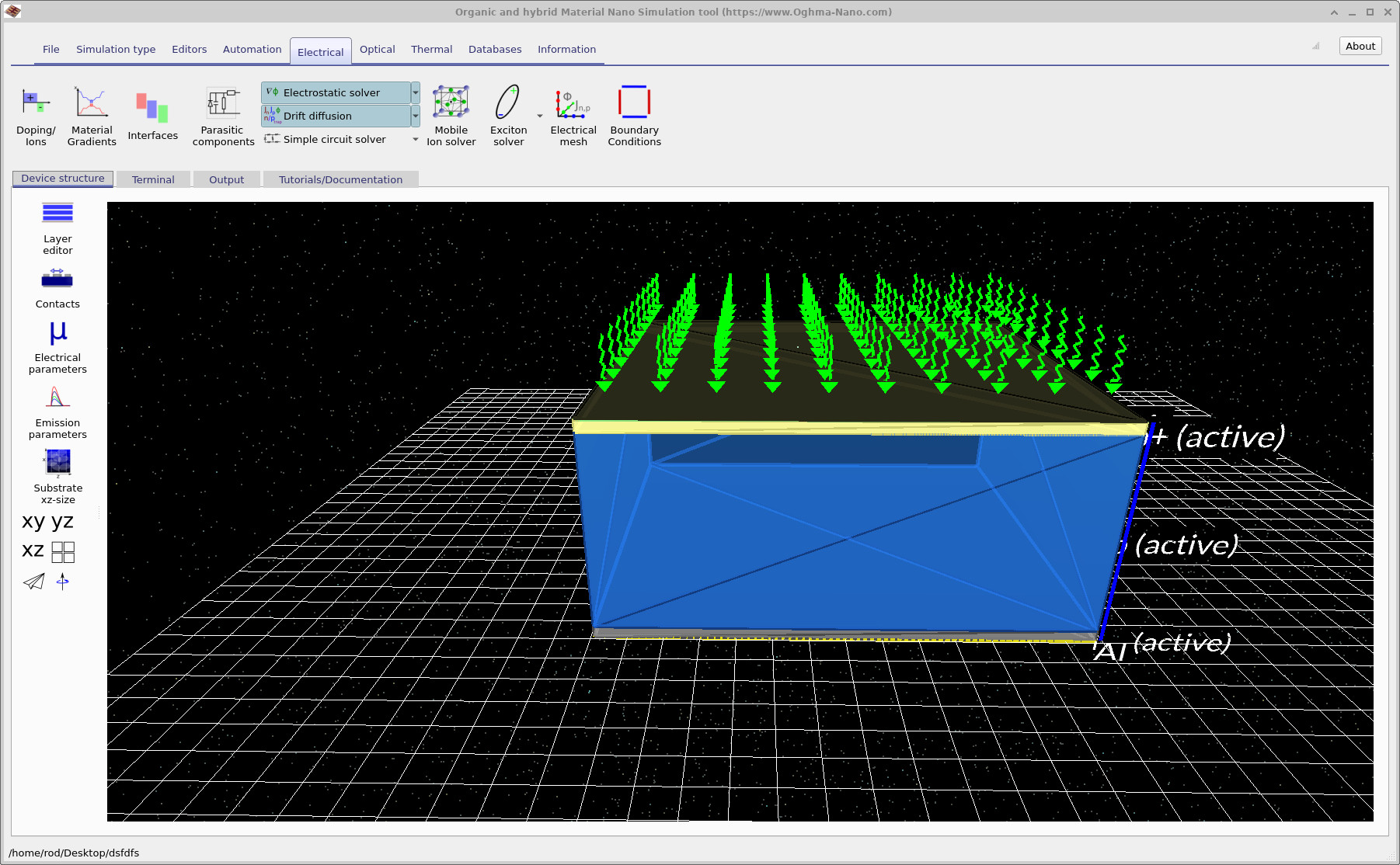
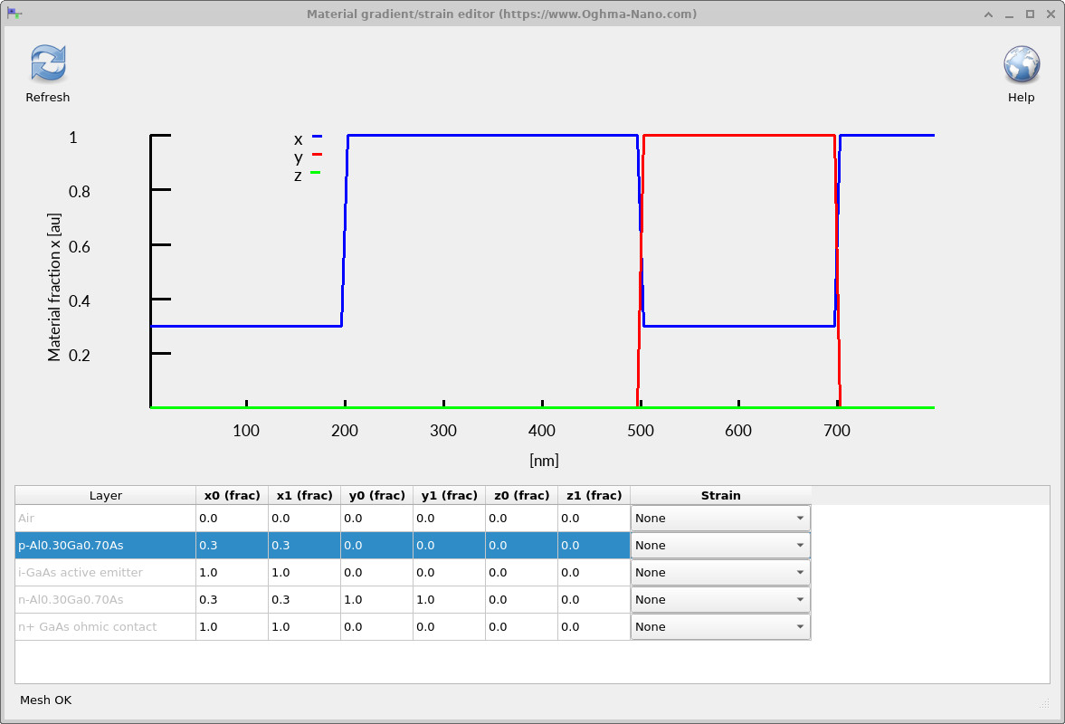
The Material gradient/strain editor lets you define alloy composition fractions for each layer and specify whether a layer should be treated as strained relative to another layer. Open the editor from the Electrical ribbon by clicking Material Gradients, as shown in ??. The editor, shown in ??, displays a plot of the composition profiles above a table of editable values.
2. Editor parameters
The table contains one row per device layer. All composition fractions are dimensionless: for example, a value of 0.30 means a fraction of 30%, not 0.30%. The columns are:
- Layer — the layer name, used to identify the part of the structure being edited.
- x0 and x1 (frac) — the value of the first alloy-composition variable at the start and end of the layer.
- y0 and y1 (frac) — the corresponding start and end values of the second composition variable.
- z0 and z1 (frac) — the start and end values of the third composition variable.
- Strain — a dropdown that specifies the reference layer relative to which the current layer is strained. Selecting None leaves this strain relationship unset.
The symbols x, y and z in this window are alloy-composition variables, not the spatial coordinates of the device mesh. Their physical meaning depends on the material model selected for the layer. Some materials use only x; more complex alloys may use additional variables. A value shown for a binary material such as GaAs should not be interpreted as an aluminium fraction unless its material model defines it that way.
3. Material composition gradients
A material gradient is a gradual change in alloy composition through a semiconductor layer. For example, in the ternary alloy \(\mathrm{Al}_{x}\mathrm{Ga}_{1-x}\mathrm{As}\), the aluminium fraction \(x\) controls the relative amounts of aluminium and gallium. Choosing \(x=0.30\) gives \(\mathrm{Al}_{0.30}\mathrm{Ga}_{0.70}\mathrm{As}\). Changing the composition changes material properties such as the band gap and band-edge energies, provided these dependencies are defined in the selected material model.
In the GaAs/AlGaAs structure in ??, the p-Al0.30Ga0.70As and n-Al0.30Ga0.70As layers both have x0 = x1 = 0.30. Their aluminium content is therefore constant through each layer. The adjacent GaAs layers form heterointerfaces with the AlGaAs layers; the displayed composition values for GaAs are interpreted according to the GaAs material model rather than as an AlGaAs alloy fraction.
To create a graded AlGaAs layer, set its start and end fractions to different values. For example, x0 = 0.20 and x1 = 0.40 describe a layer that changes from \(\mathrm{Al}_{0.20}\mathrm{Ga}_{0.80}\mathrm{As}\) at one side to \(\mathrm{Al}_{0.40}\mathrm{Ga}_{0.60}\mathrm{As}\) at the other. The fraction is interpolated linearly through the layer thickness:
\[ x(s) = x_0 + (x_1-x_0)s, \qquad 0 \leq s \leq 1, \]
where \(s\) is the normalized position through the layer, from its start (\(s=0\)) to its end (\(s=1\)). The same start/end convention applies to the y and z fractions. If both values are equal, that composition variable is uniform. Grading can be useful for tailoring band-edge profiles, reducing abrupt changes in material properties and studying carrier transport across heterostructures.
4. Strain and reference layers
Strain occurs when a semiconductor layer is forced to adopt lattice dimensions different from those it would have as a free-standing crystal. This commonly happens when a thin epitaxial layer is grown on a material with a different natural lattice constant. If the layer remains coherently attached to the underlying crystal, its in-plane lattice spacing can be stretched or compressed to match that crystal.
The Strain dropdown in the editor specifies which other layer acts as the reference for that mismatch. To model a strained layer, select the reference layer from its dropdown; the strain of the current layer is then evaluated relative to the selected layer, where supported by the material and electronic-structure models. Selecting None means that no reference-layer strain has been requested.
For a thin, coherently strained cubic semiconductor layer, the in-plane lattice mismatch can be illustrated by
\[ \varepsilon_{\parallel} \approx \frac{a_{\mathrm{ref}}-a_{\mathrm{layer}}}{a_{\mathrm{layer}}}, \]
where \(a_{\mathrm{layer}}\) is the natural lattice constant of the layer and \(a_{\mathrm{ref}}\) is that of the reference material. A positive value corresponds to in-plane tensile strain and a negative value to compressive strain. This is an explanatory lattice-mismatch relation, not a statement that the editor solves mechanical relaxation or dislocation formation.
This option is particularly useful for quantum-well structures. For example, an InGaAs quantum well grown coherently within GaAs barriers may be strained relative to the GaAs lattice. Selecting a GaAs barrier as the reference layer defines that relationship. Strain can change conduction- and valence-band energies and can split valence bands, affecting the electronic and optical properties calculated by models that include these effects. By comparison, AlGaAs/GaAs structures are relatively closely lattice matched, so their strain effects are often much smaller.
5. How they are applied
The composition fractions provide inputs to the material-property models. Where composition-dependent data are available, a graded alloy can produce position-dependent electronic properties, including band gaps, band offsets and related transport parameters. The composition profile is defined within the existing layer geometry; changing it does not alter the physical layer thickness or move the interfaces.
Strain is a separate input. Where supported, the selected reference layer allows strain-dependent electronic-structure calculations to account for the lattice mismatch between materials. This is especially important when interpreting quantum-well energy levels and optical transitions. The actual influence of a gradient or strain setting depends on the material database and the physical model used in the simulation: entering a fraction does not, by itself, guarantee that every material property changes with composition.
6. Practical workflow
- Choose the layer materials in the layer editor, including any ternary or multicomponent alloys that require composition fractions.
- Open Electrical → Material Gradients and locate the relevant layer in the table.
- Enter equal start/end fractions for a uniform alloy, or different values to create a linear composition gradient. Use only the composition variables supported by that material's model.
- If the layer should be strained, use its Strain dropdown to choose the appropriate reference layer. Otherwise leave it at None.
- Use Refresh to update the plot, then check that the fraction profiles agree with the intended device structure.
For the GaAs/AlGaAs example shown here, the AlGaAs layers are set to x0 = x1 = 0.30, giving uniform 30% aluminium composition. To investigate an alloy-grade effect, change one of these start/end values and compare the resulting band profile. To investigate a strained quantum well, select its surrounding reference layer in the Strain column and use an electronic-structure model that supports strain.