Parasitic components editor
1. Overview
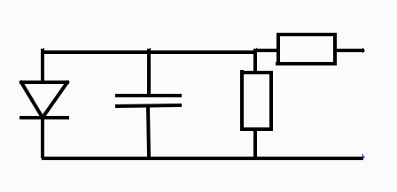
Real devices rarely behave like ideal diodes. Series resistance from electrodes and wiring, leakage through imperfect insulation paths, and “extra” dielectric thickness from encapsulation or buffer layers all modify the measured response. The Parasitic components editor lets you account for these effects when simulating two-terminal devices (e.g., OLEDs/LEDs, solar cells, photodiodes). The parameters are automatically included when generating JV curves and related plots.
2. Parameters
The editor exposes three quantities:
- Shunt resistance (Ω·m²) — an area-normalized leakage path across the device. Using units of Ω·m² keeps the dark JV curve invariant with respect to device area: if the simulated area changes, the absolute shunt current scales correctly so the current density remains unchanged.
- Series resistance (Ω) — a lumped resistance in series with the device (e.g., ITO sheet resistance, wiring, contacts). Specified in ohms because it is intuitive to conceptualize as a total series element.
- Other layers (m) — an effective additional thickness, \(\Delta t\), that adjusts the geometric capacitance to account for extra dielectric spacing (encapsulation, spacers, etc.).
3. How they are applied
For two-terminal devices (OLEDs/LEDs, solar cells, photodiodes and similar), these parameters are included automatically in the simulated JV characteristics and small-signal responses. For devices with more than two terminals (e.g., OFETs and other transistor-like or complex multi-terminal structures), it is not obvious at which terminals to apply a single pair of series/shunt elements; therefore these parasitic parameters are not applied automatically. In such cases, add equivalent parasitics in post-processing according to your chosen measurement configuration.
Geometric capacitance with “Other layers”. In practice, the experimentally measured geometric capacitance of a device does not always match the value predicted by the simple dielectric slab formula. This discrepancy can arise for several reasons: field-line leakage at the edges, electrodes that are slightly larger or smaller than assumed, inaccuracies in the actual device thickness, or uncertainty in how to treat multiple semiconductor layers (particularly when some of them can hold charge).
To allow the user to account for these effects, OghmaNano introduces an additional parameter, Other layers, which acts as an effective thickness correction \(\Delta t\). By default, this parameter is set to zero, so unless the user explicitly modifies it, the capacitance is calculated from the nominal device geometry.
\[ C_{\mathrm{geo}} \;=\; \frac{\varepsilon A}{d + \Delta t}, \]
where \(d\) is the nominal device thickness, \(A\) is the device area, and \(\varepsilon = \varepsilon_0 \varepsilon_r\) is the permittivity. By adjusting \(\Delta t\), the user can bring the simulated geometric capacitance closer to the experimentally observed value, compensating for uncertainties in device geometry, contact definition, or field distribution. This correction is primarily relevant in transient simulations (e.g., charge/discharge dynamics) and frequency-domain calculations (e.g., impedance spectroscopy), where the precise value of the capacitance strongly influences the simulated response.