Layer editor
1. Overview
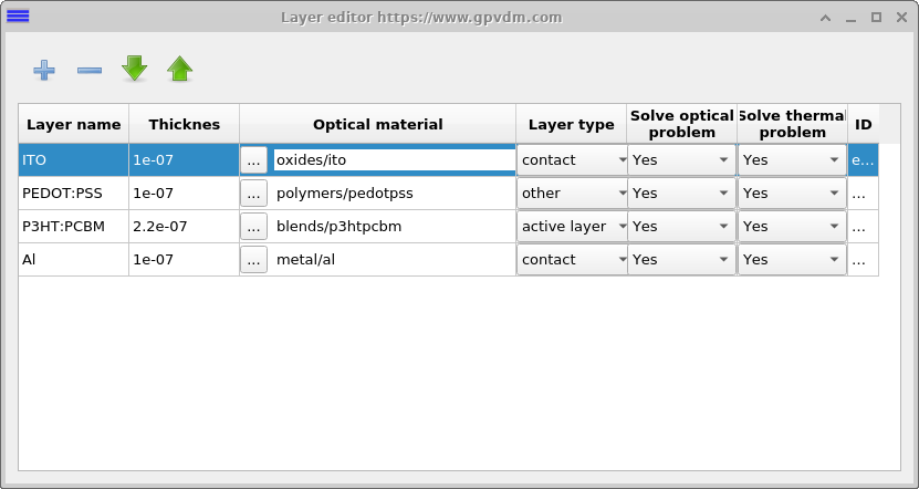
Almost all optoelectronic devices, including solar cells, OLEDs, and OFETs are built from a sequence of material layers. In inorganic devices these layers are often fabricated using methods such as vacuum deposition, while in organic and hybrid devices techniques such as spin coating or printing are used. In OghmaNano this layered structure is represented in the Layer editor, which provides an interface for defining and modifying the epitaxy of a device. The term epitaxy originates from inorganic semiconductor physics but in OghmaNano it simply refers to the ordered stack of layers that make up a device.
2. Defining a layer
The Layer editor displays the device as a table of layers. Each row contains:
- Layer name — the label used to identify the layer.
- Thickness — the physical thickness of the layer.
- Optical material — the material database entry providing refractive index and absorption data.
- Layer type — whether the layer is a Contact (contact), Electricaly active (active) , Not electricaly active (other)
- ID — the far-right column contains the layer’s unique ID (the object identifier from the project’s JSON). You can expand this column to reveal the full value and copy it. Use this ID when writing scripts or searching the JSON to unambiguously reference a specific layer—even if its human-readable name changes.
3. Layer types
Each layer in a device must be assigned a layer type, which determines how it is treated in the simulation. There are three possible types:
- Contact — defines electrical contacts at the boundaries of the device (typically the top and bottom). These act as current extraction points and impose the boundary conditions used by the electrical solver.
- Active — designates a semiconducting layer in which both electrons and holes are present, and where drift–diffusion and Poisson’s equations are be solved. This is where charge transport, recombination, and generation occur.
- Other — covers all remaining layers, such as transport layers, buffer layers, or encapsulation. These layers will be considered by the optically and thermal model but not by the drift-diffusion solver.
It’s a common mistake to want to solve the drift–diffusion equations in every layer of the device. In practice this is unnecessary: many layers are single-carrier or highly conductive—for example, hole-transport (HTL) and electron-transport (ETL) layers in organic devices—so electron–hole recombination and related charge-pair dynamics do not occur there. Solving drift–diffusion in such regions increases computational cost without adding physical insight. Use the active layer flag only when you absolutely must solve the coupled drift–diffusion and Poisson equations—for example, in the photoactive layer of a solar cell, the channel of an OFET, or any region where both electrons and holes coexist and their transport/recombination must be modeled explicitly. Layers such as HTL/ETL, highly conductive buffers, or metal contacts usually should not be marked as active unless one wants to study effects such as S-shaped JV curves in solar cells.