OPV Contacts: Ohmic, Schottky and Boundary Conditions
This section explains how OPV contacts define the electrical boundary conditions used in solar-cell simulations. Contact polarity, majority carrier type, bias mode, charge density and the choice of ohmic or Schottky model all influence charge extraction, JV curves and the open-circuit voltage.
1. OPV contact editor and boundary conditions
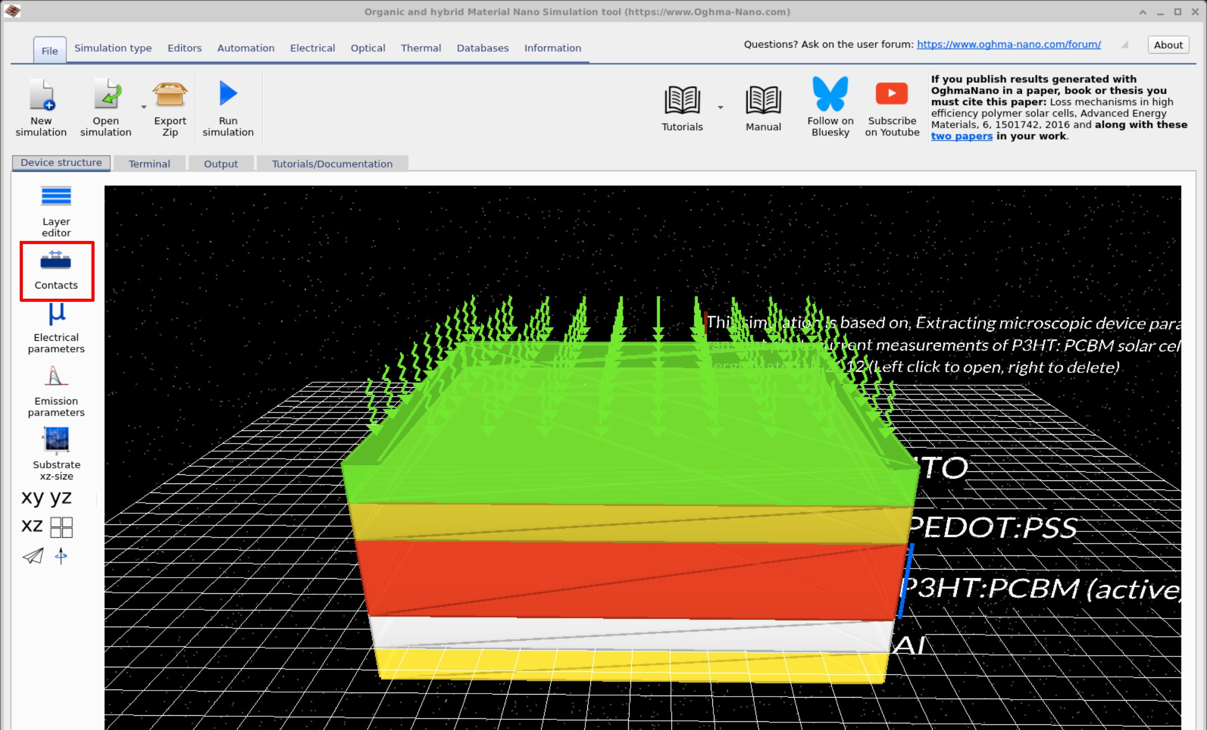
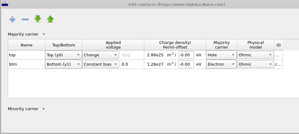
Every device needs contacts — they are how voltage is applied and current is collected. In OghmaNano, contacts are configured in the Contact editor, opened from the main window by clicking the Contacts button (see ??). This opens the editor window shown in ??, where you set both geometry (which side of the device) and electrical properties (biasing, majority carrier, model).
2. Contact editor fields: bias mode, carrier type and contact model
- Name — A descriptive label for the contact (no physical effect on the simulation).
- Top/Bottom — The physical placement of the contact on the device stack. For 2D geometries, left/right placements are also supported (introduced later).
- Applied voltage — Select how this contact is driven during a simulation:
- Ground: Forces the contact to 0 V (reference).
- Constant bias: Holds the contact at a specified fixed voltage.
- Change: Marks this contact as the one to be swept/perturbed (use this for JV sweeps or for the driven terminal in impedance spectroscopy / time-domain studies).
- Charge density / Fermi offset — Sets the majority charge density at the contact, which determines the local Fermi-level offset and effectively how “good” (selective/ohmic) the contact is. As a rule of thumb, higher majority charge density generally yields a lower-resistance, more selective contact.
- Majority carrier — Choose whether the contact predominantly conducts electrons or holes. For a non-inverted P3HT:PCBM device, the anode (e.g., ITO/PEDOT:PSS, top in this example) is hole-selective, while the cathode (e.g., Ca/Al, bottom) is electron-selective.
- Physical model — The transport boundary condition at the contact:
- Ohmic (recommended starting point): Assumes efficient injection/collection for the chosen majority carrier.
- Schottky: Includes barrier-limited transport; useful when studying blocking contacts and VOC losses.
Tip: When running a JV sweep, set one contact to Change and keep the other at 0 V. For studies of contact-limited VOC, try lowering majority charge density or switching to a Schottky model to observe how non-ideal selectivity reduces the open-circuit voltage.
3. Contact carrier density and JV performance
Show suggested answer
For ohmic contacts, the majority carrier density defines the availability of states at the interface. Lower values effectively increase the contact resistance and reduce the efficiency of carrier exchange.
- VOC: Can decrease slightly due to enhanced recombination at the contact, since carriers are less efficiently extracted.
- FF: Typically drops, showing increased curvature or roll-off in the JV curve from contact-limited transport.
- JSC: Usually less affected at first, but can decrease if extraction becomes severely limited at low carrier density.
- PCE: Declines mainly due to FF (and sometimes VOC) losses.
Physically, this is akin to moving from an ideal ohmic contact toward a resistive one: the contact still injects/extracts the correct carrier type, but with less efficiency.
📝 Check your understanding (Part F – Contacts)
- In the Contact editor, which fields set (a) the driven terminal for a JV sweep and (b) the reference terminal?
- Explain the difference between Ground, Constant bias, and Change. When would you use each?
- What does the Majority carrier setting do, and how should it be configured for a non-inverted P3HT:PCBM device?
- Describe the practical difference between the Ohmic and Schottky contact models. How might each influence VOC?
- How can reducing the majority charge density at an ohmic contact affect the JV curve (JSC, VOC, FF)? What physical effect is this mimicking?
- If only one contact is set to Change for a JV sweep, what should the other contact be set to, and why?
- Which contact collects electrons and which collects holes in a standard (non-inverted) P3HT:PCBM cell, and how does misconfiguring this show up in the JV?
👉 Next step:
- Return to the introduction to organic electronics for a broader overview of organic device simulation.