OPV Parasitic Resistance: Series, Shunt and Dark JV Simulation
This section explains how parasitic resistance affects organic solar-cell simulations. Series resistance, shunt resistance and dark JV curves are useful diagnostic tools because they separate contact losses, leakage paths and recombination-dominated regions of the device response.
1. Series resistance, shunt resistance and the OPV JV curve
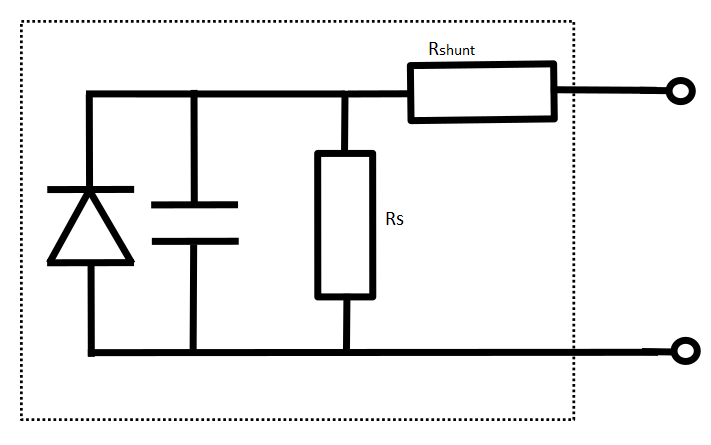
Drift–diffusion simulations describe the photoactive layer in detail, where electrons and holes are both present and interact. Real devices, however, also include non-ideal effects introduced by the contact layers and fabrication imperfections. One important effect is the series resistance (Rs), a lumped resistance in series with the diode that arises from contacts, transport layers (HTL/ETL), and wiring or sheet resistance. It produces the characteristic high-bias “roll-off,” limiting the current at large forward voltages and reducing the fill factor.
A second effect is the shunt resistance (Rshunt), a leakage path in parallel with the active layer. This is caused by imperfections such as pinholes, impurities, edge leakage, or micro-shorts that create unintended conductive pathways through the device. It mainly degrades the low-bias region of the JV curve, reducing the slope near the origin and lowering JSC and fill factor.
These contributions are usually referred to as parasitic components and can be represented in a compact circuit model, shown in ??. In this model, the ideal diode (governed by the drift–diffusion equations) appears in parallel with Rshunt and in series with Rs. A parasitic capacitor is also included to represent the geometric capacitance of the contacts; this term is only relevant in transient simulations.
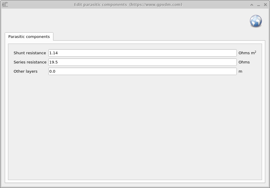
You can edit parasitic components in OghmaNano by going to the Electrical ribbon in the main window and selecting Parasitic components. This opens the Parasitic component editor, where you can set both the shunt and series resistances. This can be seen in ?? Shunt resistance (Rshunt) is entered as an area-normalised value (Ω·m2). This ensures that the effective shunt resistance scales with device area. Series resistance (Rs) is specified in ohms (&Omega) as a lumped resistance, independent of device area. Together, Rshunt and Rs allow you to capture real-world leakage and conduction losses in addition to the drift–diffusion physics of the active layer.
2. Dark JV simulation and resistance extraction
Up to now, all simulations have been run in the light under AM1.5G illumination. This is natural, since we are usually interested in how much power a solar cell can generate. However, measuring a device in the dark often reveals even more about its internal physics — and why it may not be performing as expected. A common mistake is to characterise a new device only under illumination; in fact, the dark JV curve can provide richer diagnostic information than the light curve.
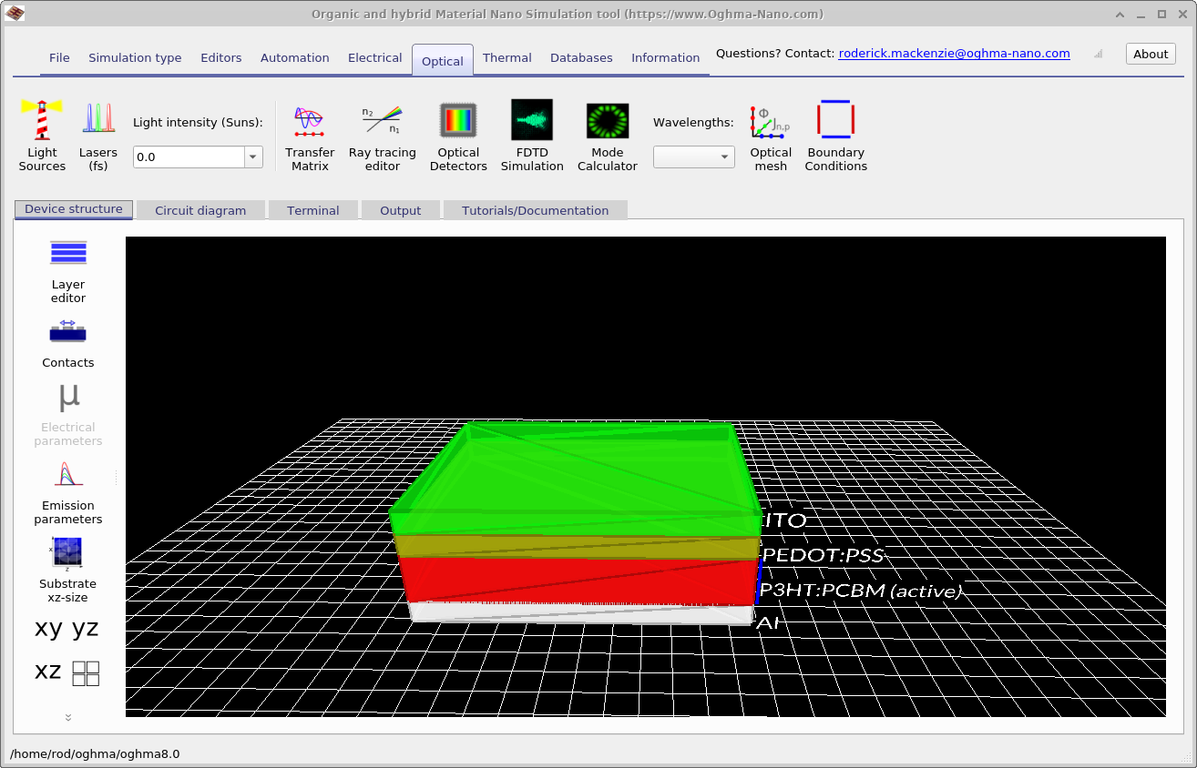
In this section we will use the dark JV to investigate how Rshunt and Rs can be extracted. To begin, switch the simulator into darkness: go to Optical ribbon → Light intensity (suns) and set the value to 0.0. The green photons in the 3D device view will disappear, confirming that the simulation is running without illumination. This can be seen in ??.
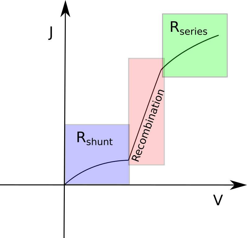
Next we will explore how parasitic resistances shape the dark JV. Start by setting Rshunt to a high value (e.g. 1 MΩ·m²) and run a JV sweep, then reduce it to a much lower value (e.g. 1 Ω·m²) and compare the curves. Observe how the slope at low voltages is affected by shunt leakage. Then repeat the process for the series resistance: set Rs first to 0 Ω, then to a larger value (e.g. 20 Ω). Compare the high-voltage region of the JV curve and note how the roll-off changes. Plot each case on x-linear / y-log axes (press l) so the differences are clearly visible. ?? plots how the resistances should affect the different parts of the JV curve. Note that changing only the parasitic resistances does not directly alter the recombination-dominated region; that is controlled by the electrical material parameters discussed in Part E.
📝 Check your understanding (Part D)
- What physical effects are represented by Rshunt and Rs in the equivalent circuit of a solar cell?
- How does a low Rshunt value change the slope of the JV curve at low voltage?
- How does a large Rs value affect the JV curve at high voltage and the fill factor?
- Why is it useful to plot dark JV curves on x-linear / y-log axes, and what additional insight does this provide?
- What does the “Other layers” term (Δ) in the capacitance expression account for physically?
- When extracting Rshunt and Rs from a dark JV, which regions of the curve should you analyse?
👉 Next steps:
- Continue to Part E: Electrical parameters to explore mobilities, traps, and other core device settings.
- Return to the introduction to organic electronics for a broader overview of the topic.