OPV Device Structure: Layer Editing, Active Layers and Thickness
Before attempting this section, make sure you have completed Part A and Part B.
1. Editing the OPV device structure
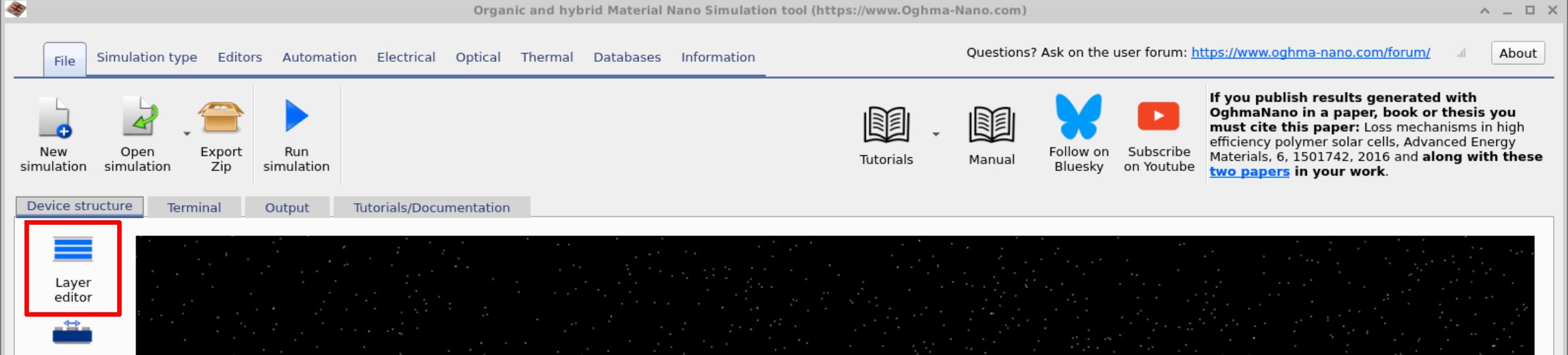
Organic solar cells are multilayer devices, and the OPV device structure strongly affects optical absorption, charge extraction and simulated performance. In OghmaNano, the Layer editor is used to define the solar-cell stack, including layer thickness, optical material and whether each layer is treated as active, contact or other. This editor can be opened from the main simulation window under the Device structure tab, as shown in ??. The Layer editor itself is shown in ??.
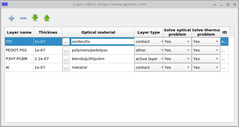
The Layer editor window displays a table describing the device structure. Each row corresponds to a layer, with columns for properties such as name, optical material, type, and Thickness, which sets the physical thickness of the layer. In this example, the P3HT:PCBM layer is the active layer — the part of the device that absorbs photons and generates charge carriers (electrons and holes).
2. Active-layer thickness and OPV performance
An active-layer thickness of about 50 nm is considered thin for an OPV, while 400 nm is relatively thick. A thicker layer absorbs more light, but it also increases the distance that photogenerated charges must travel to reach the contacts. As the distance they travel grows, so does the probability of a photogenerated electron meeting a photogenerated hole (recombination). This reduces the fraction of carriers that can be successfully extracted. Consequently, device performance does not improve indefinitely with increased absorption. Thus, there is always a trade-off between absorbing all the light by making the device thick, and not making the device too thick so that the carriers have a good chance of escaping the device. This trade-off is a central principle in OPV design.
3. Layer editor fields
The Layer editor has the following columns:
- Layer name: A plain-text name for the layer. You can call layers anything you like (e.g. ITO, PEDOT, Fred, or Bob); the name itself has no physical meaning.
- Thickness: The layer thickness, specified in meters.
- Optical material: Specifies the n/k dataset used to describe the material’s optical properties. These values come from experimental data stored in the optical database (??) and are independent of electrical properties such as band gap.
- Layer type: Defines how the simulator treats the layer:
- active: An electrically active layer where the drift–diffusion solver solves the electrical equations (??). You may have multiple active layers, but they must be contiguous.
- contact: A layer defined as an electrode where a voltage is applied. See ?? for details.
- other: Any layer that is neither a contact nor active. These are treated as passive layers.
4. Which OPV layers should be active?
A common mistake when defining a device structure is to assume that all layers must be set as active simply because every layer conducts current. In reality, most transport or contact layers only conduct one type of carrier (either electrons or holes) and behave effectively like resistors. For example, in a standard P3HT:PCBM solar cell the PEDOT:PSS layer conducts only holes, while the Ca/Al contact conducts only electrons. Solving the full drift–diffusion equations (for both carrier types) in such layers does not make physical sense.
Active layers should therefore be restricted to regions where both carriers are present and where photogeneration, recombination, or trapping occurs. In OPVs, this means the bulk heterojunction (BHJ); in perovskite solar cells, the perovskite absorber. These are the layers in which the full device physics must be solved.
There are exceptions. For instance, if you wish to study the impact of poor or blocking contacts (leading to effects such as S-shaped JV curves), or if multiple layers genuinely host both carriers (e.g. in OLEDs), you may designate additional layers as active. However, as a general rule, keep the number of active layers to a minimum. This keeps simulations simple, efficient, and the underlying physics easier to interpret.
📝 Check your understanding (Part C)
- Which field in the Layer editor controls whether a layer is treated as active, contact, or other?
- Why is the P3HT:PCBM layer set as active, while layers such as PEDOT:PSS and Ca/Al are not?
- What physical trade-off occurs when increasing the thickness of the active layer from 50 nm to 400 nm?
- If you wanted to investigate S-shaped JV curves caused by poor contacts, how might you change the layer definitions?
- In an OPV simulation, which output file contains the device performance summary values (JSC, VOC, FF, PCE)?
- Give one example of a situation where more than one active layer might be appropriate (hint: think about OLEDs).
👉 Next steps:
- Continue to Part D for electrical parameters.
- Return to the introduction to organic electronics for a broader overview of the topic.