OPV Electrical Parameters: Mobility, Recombination and μτ Product
This section explains how OPV electrical parameters control charge transport and recombination in organic solar-cell simulations. Carrier mobility, bimolecular recombination, SRH traps, carrier lifetime and the μτ product determine how efficiently photogenerated charges are extracted before they recombine.
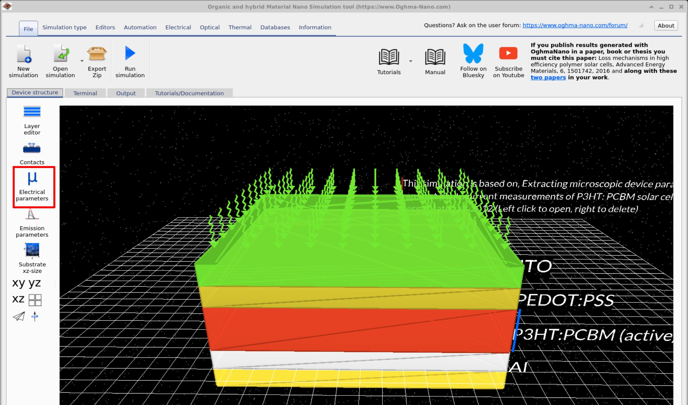
1. OPV electrical parameter editor
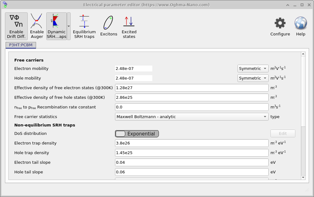
You can access the electrical parameter editor by clicking the Electrical parameters button in the main interface (see ??). Once open, the editor allows you to adjust mobilities, recombination constants, trap models, and other processes associated with active layers. This window is shown in ??. Any layer set as active in the Layer editor will appear here.
The toolbar at the top enables or disables specific physical mechanisms — pressing a button switches the mechanism on:
- Drift–diffusion: Normally enabled for any active layer.
- Auger recombination: Rarely used in OPV devices, but available for study (??).
- Dynamic Shockley–Read–Hall (SRH) traps and Equilibrium SRH traps: Used to describe recombination via trap states. By default these are enabled in organic simulations (??).
- Excitons (diffusion) and Excitons (singlet/triplet): Used to describe excited states. These are discussed later (??).
2. SRH traps and bimolecular recombination
In most organic simulations, Dynamic Shockley–Read–Hall (SRH) traps are enabled by default because trap-mediated recombination is common in disordered materials and often dominates the recombination landscape. For this introductory example, however, SRH adds unnecessary complexity, so we will temporarily disable it.
To turn SRH off, click the Dynamic SRH traps button once on the toolbar. The associated SRH fields will disappear from the Electrical parameter editor (see ??). You can re-enable SRH at any time by clicking the button again.
A recombination pathway must still be present—otherwise electrons and holes would live indefinitely—so for this exercise we will use free-to-free (bimolecular) recombination. In the Electrical parameter editor, set the nfree → pfree recombination rate constant to 1 × 10⁻¹⁵ m3·s−1. This simple model describes one free electron recombining with one free hole. While it is not a perfect description for organic semiconductors, it is sufficient for the purposes of this example. The bimolecular (free-to-free) recombination rate is given by:
R(x) = k · n(x) · p(x)
where R(x) is the recombination rate, k is the bimolecular recombination constant, and n(x), p(x) are the local electron and hole densities.
3. Mobility, recombination, lifetime and the μτ product
Two of the most important parameters for device performance are the carrier mobility (μ) and the free-to-free recombination constant (k). In OghmaNano, these are set in the Electrical parameter editor: the Electron mobility and Hole mobility fields control μ, while the nfree → pfree recombination rate constant field defines k (see ??).
Mobility determines how quickly charge carriers drift through the device: higher μ means carriers reach the contacts faster, reducing the chance of recombination. Recombination between free carriers (an electron and a hole meeting) sets the carrier lifetime (τ). A large recombination constant k means carriers recombine quickly, giving a short τ, while a small k means carriers survive longer. In a simple picture, the lifetime can be related to the carrier density and recombination constant as:
τ ≈ 1 / (k · n)
where n is the carrier concentration. This shows that higher recombination constants or higher carrier densities both lead to shorter lifetimes, while smaller values extend τ and improve the probability of carrier extraction.
Together, mobility and lifetime form the μτ product (μ·τ), which expresses how far a carrier can travel before recombining. A larger μτ increases the probability that a photogenerated carrier escapes to the contacts and contributes to useful current. In practice, μτ is a convenient figure of merit for the transport–recombination “quality” of a solar cell: devices/material stacks with higher μτ generally tolerate thicker active layers and exhibit improved carrier collection (often reflected in higher JSC and FF). It is not a complete descriptor—optical absorption, energetic offsets, and contact selectivity also matter—but it provides a quick way to compare device quality across materials and processing conditions.
4. How to choose OPV electrical parameters
For traditional semiconductors such as AlGaAs or InP, the values of carrier mobilities, band gaps, and recombination constants are well tabulated in the literature. These materials are produced at extreme purities (often “eleven nines,” or 99.999999999%), which means their physical properties are highly reproducible. If you have a wafer of GaAs, you know almost exactly what its mobility or lifetime will be, and you can simply look them up in a reference book (e.g. Piprek’s Semiconductor Optoelectronic Devices).
Novel semiconductors such as organics or perovskites are very different. Their purity is typically only around 99.9% at best — eight orders of magnitude less pure than traditional III–V semiconductors. They are also structurally disordered: instead of atoms packed into a regular lattice, organics form a tangled collection of polymers and molecules, while perovskites often form heterogeneous domains. Because their morphology depends strongly on fabrication conditions, the “same” material from the same supplier can behave very differently depending on who deposited it, where, and how. As a result, electrical parameters like mobility, trap density, and recombination constants cannot simply be looked up: they must be estimated, tuned, or fitted to experimental data.
So, what should you do when setting parameters for a novel device? Practical guidance:
- Start with base simulations: The example files provided in OghmaNano are calibrated to experimental devices or use sensible literature values.
- Consult the literature: Search for studies on similar materials to establish reasonable parameter ranges (mobilities, lifetimes, trap densities, recombination constants).
- Compare to experiment: Run a simulation and check whether the JV magnitudes are in the same ballpark as experiment. If they are far off, adjust mobilities or recombination constants.
- Fit to data (advanced): Direct parameter extraction by fitting to experimental JV curves is possible (??), but this is challenging and should not be your first approach.
📝 Check your understanding (Part E)
- Which fields in the Electrical parameter editor set (a) electron mobility, (b) hole mobility, and (c) the free-to-free recombination constant?
- What physical processes do Dynamic SRH traps represent, and why did we turn them off for this example?
- Write the expression for the bimolecular recombination rate R(x) in terms of k, n(x), and p(x).
- How is carrier lifetime (τ) related to the recombination constant k and carrier density?
- What does the μτ product represent physically, and why is it considered a useful figure of merit for solar cells?
- If you increase electron and hole mobilities by two orders of magnitude, what change would you expect in carrier extraction and device efficiency?
- When comparing simulations with SRH recombination and with free-to-free recombination, why might the JV curves differ slightly even though both describe carrier loss?
- Why can parameters like mobility or recombination constants be looked up for traditional semiconductors (e.g. GaAs, InP), but must often be estimated or fitted for organics and perovskites?
👉 Next steps:
- Continue to Part F: Contacts and VOC to explore how contact properties influence the open-circuit voltage of OPVs.
- Return to the introduction to organic electronics for a broader overview of the topic.