OPV Optical Simulation: Sunlight, Absorption and Generation
This section explains how optical simulation is used to model sunlight absorption and charge generation in organic solar cells. In OghmaNano, OPV optical modelling combines the AM1.5G solar spectrum, wavelength-dependent material absorption, and transfer-matrix simulations to calculate where photons are absorbed in the device stack. These absorption profiles determine where electron–hole pairs are generated and therefore provide the optical input to the electrical OPV simulation.
1. Exploring OghmaNano's optical database
- Navigate to the Databases ribbon as shown in ??.
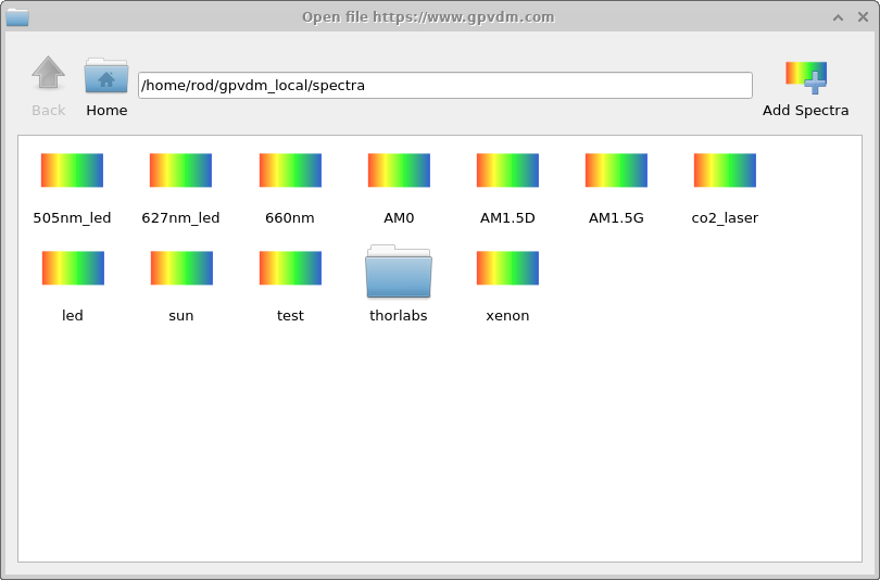
- Click the Optical database icon to open the window shown in ??.
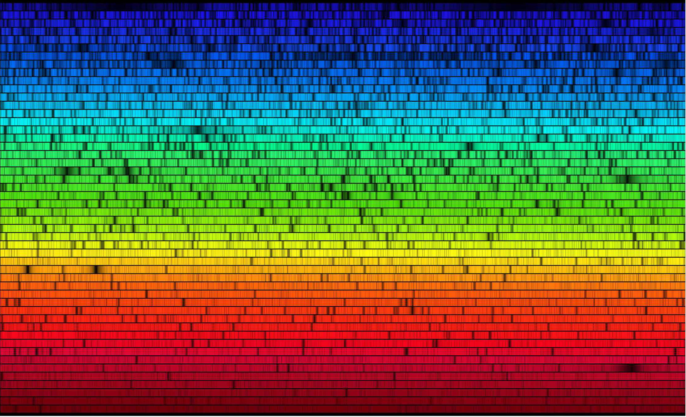
- Double-click AM1.5G to view the standard solar spectrum. Note where the irradiance is highest and look for the small atmospheric absorption dips. You should see a plot similar to ??.
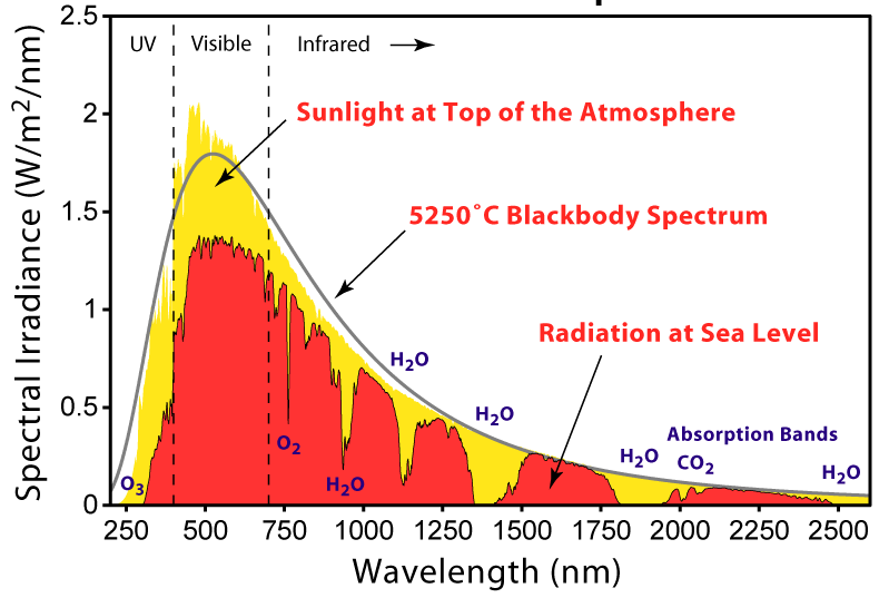
2. Exploring the AM1.5G solar spectrum
The Sun’s intensity varies throughout the day and also depends on your location in the world. To fairly compare solar cells, we therefore use a standard spectrum known as AM1.5G. Plots of this spectrum are shown in ?? and ?? (false-colour). The AM1.5G spectrum represents sunlight after it has passed through about 1.5 times the atmospheric thickness compared to the Sun directly overhead, corresponding to typical mid-latitude conditions in the afternoon. The small “dips” visible in the spectrum are due to atmospheric absorption — for example, ozone in the UV and water vapour or CO2 in the infrared. Using the AM1.5G spectrum in your simulations allows your results to be compared directly and consistently with values reported in the literature.
3. How OPV materials absorb light
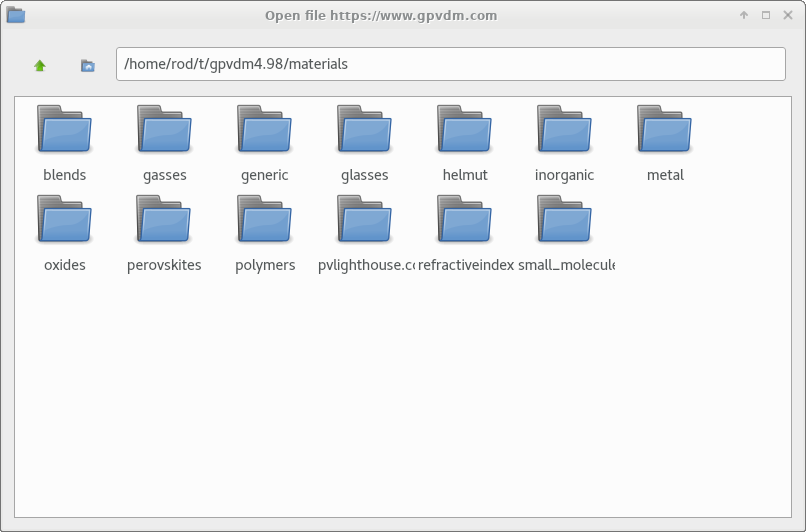
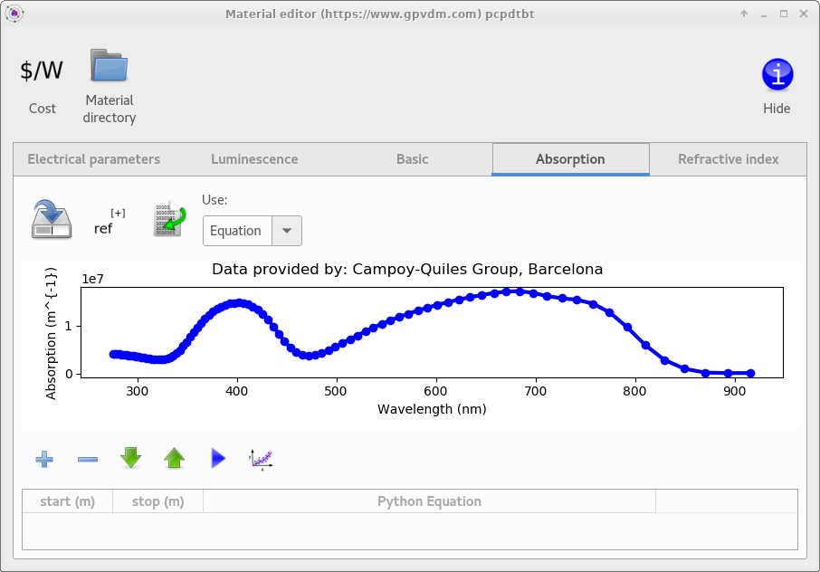
Solar cells are built from multiple layers. Some layers are designed to absorb light, others to conduct charge carriers. To inspect the optical absorption of a given material, open the Materials database, which can be accessed by clicking on the "Materials Database" icon in ??. Then navigate to polymers and open P3HT, then select the Absorption tab (??). This shows how strongly the polymer absorbs as a function of wavelength, it is important to note that all materials absorb light differently at different wavelengths.
polymers.
The solar spectrum is a continuous spectrum of wavelengths; different wavelengths of light interact with the device in different ways, these are described below:
- UV (≈200–400 nm): Most UV-C/UV-B never reaches the device as it is absorbed in the atmosphere/glass.
- Visible (≈400–700 nm): The main working band for OPVs. After modest losses at glass/ITO, this light is absorbed in the active layer according to its absorption spectrum.
- Near-IR (≈700–2500 nm): Contains a lot of the Sun’s power, but thin organic layers absorb it weakly, much of it is reflected
- Mid/Far-IR (>≈2500 nm): This is mainly thermal radiation and is generally not useful for OPV devices.
4. Simulating light absorption and charge generation
Now that we have looked at the AM1.5G solar spectrum and how materials absorb light as a function of wavelength, we can combine these ideas and simulate photon absorption inside the device stack.
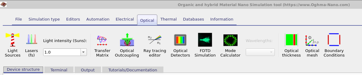
Open the Optical ribbon (Figure ??) and choose Transfer Matrix Simulation. In the window that opens, click Run optical simulation (the play button). OghmaNano will compute wavelength-resolved absorption using the transfer-matrix method.
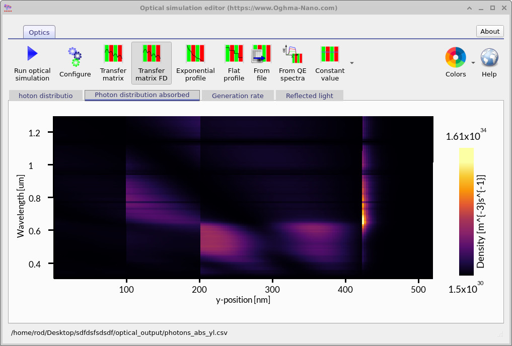
The results are shown on multiple tabs. The Photon distribution view shows the optical field throughout the stack, while Photon distribution (absorbed) visualises where photons are absorbed as a function of both position in the device and wavelength (Figure ??).
Interpreting the map: on the left side of the device there is essentially no absorption in the transparent ITO, followed by absorption within the active and adjacent layers. Any light that propagates through without being absorbed is ultimately reflected or lost at the back metal contact. The colour scale can be viewed on a logarithmic scale to highlight weak absorption features.
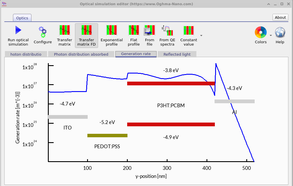
Finally, the absorbed-photon density is integrated over wavelength to produce a one-dimensional generation profile versus position (Figure ??). This plot shows where the device actually generates electron–hole pairs and helps you assess how effectively the optical design directs sunlight into the active layer.
📝 Check your understanding (Part B)
- Which standard solar spectrum is most commonly used in OPV simulations?
- What do the dips in the AM1.5G spectrum come from?
- Which part of the spectrum (UV, visible, IR) do OPV active layers mainly absorb?
- In the absorption map, why is there almost no absorption in the ITO layer?
- What does the 1D absorption profile tell you about the device?
👉 Next steps:
- Continue to Part C for a tutorial on exploring the device structure.
- Return to the introduction to organic electronics for a broader overview of the topic.