

GaInNAs Dilute-Nitride Quantum Well: 10-Band Zincblende k·p Tutorial
1. Introduction
In this tutorial we will simulate a GaInNAs dilute-nitride quantum well using OghmaNano's ten-band zincblende k·p model. We will open an existing example, inspect the layer structure, run the electronic-state calculation and examine its predicted optical spectra. The example contains a 7 nm GaInNAs quantum well within a larger GaAs/AlGaAs structure, rather than an isolated three-layer well.
Why is a ten-band model useful? Ordinary eight-band k·p theory describes a conduction band and the heavy-hole, light-hole and split-off valence bands, including spin. Introducing a small concentration of nitrogen into a III–V alloy can create a nitrogen-related resonant level that interacts particularly strongly with the host conduction band. A ten-band description adds two spin components of this nitrogen-related state. The interaction can substantially lower the fundamental transition energy and change the conduction-band curvature. This makes dilute nitrides interesting for longer-wavelength optical devices.
2. Opening the ten-band example
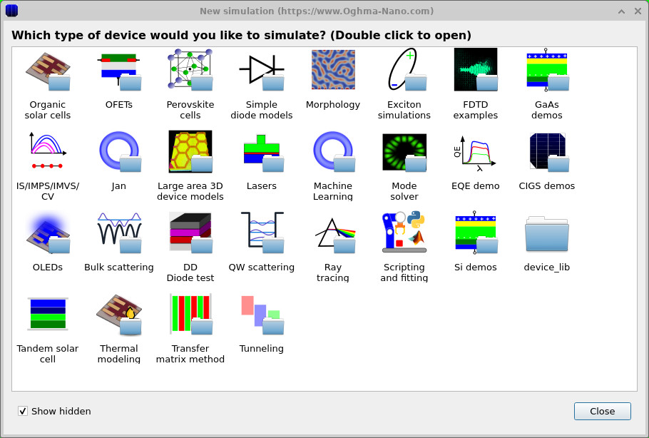
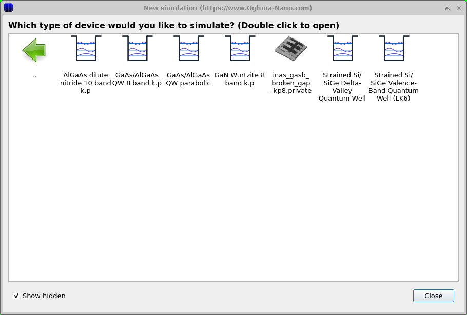
Select File → New simulation. In the new-simulation window, double-click GaAs demos (??). The next window contains several quantum-well examples. Select AlGaAs dilute nitride 10 band k.p (??). This loads the preconfigured ten-band simulation, including the appropriate layer definitions and material-parameter files.
3. Device structure and material parameters
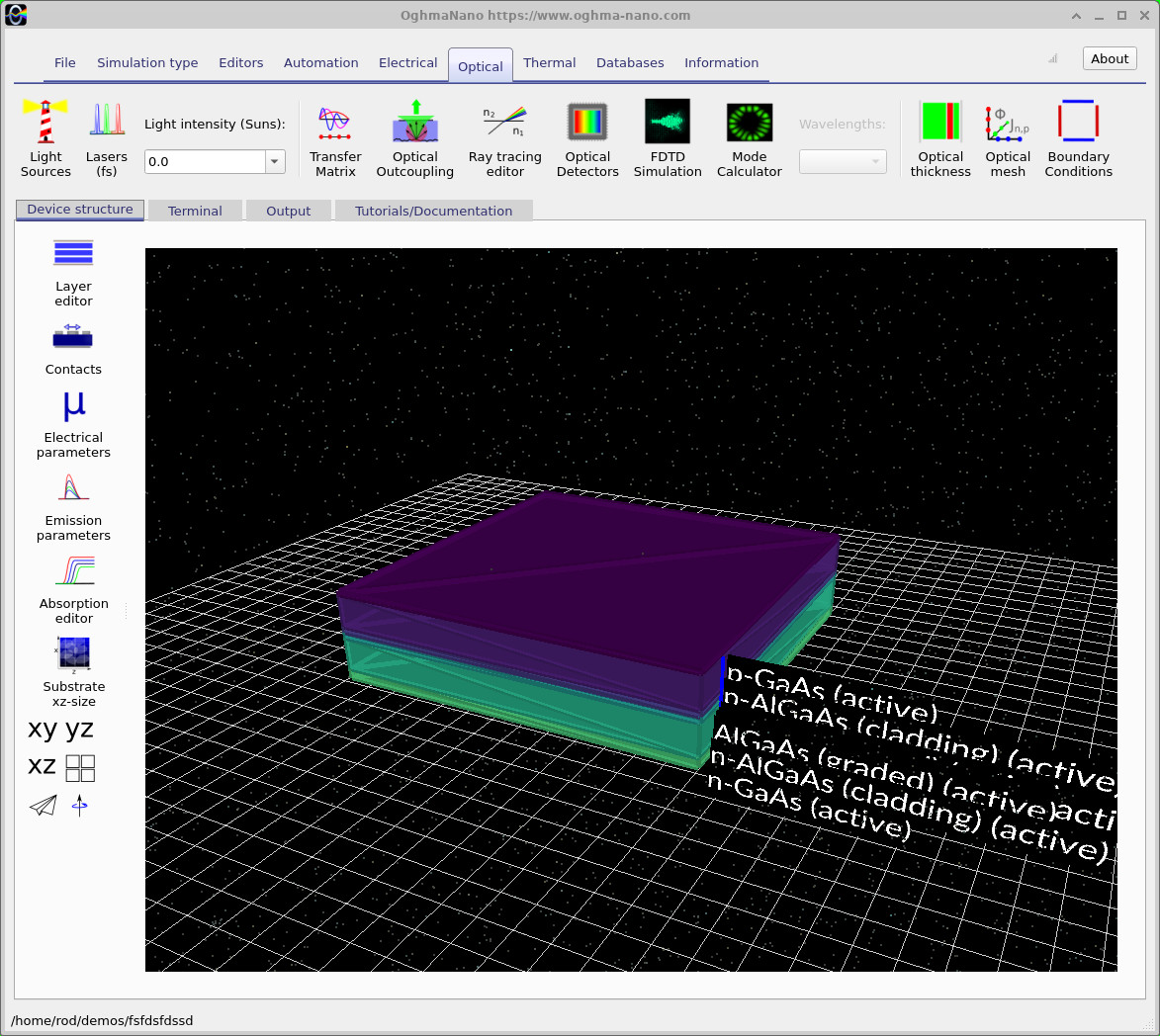
The main window displays the multilayer structure (??). Unlike the simple GaAs/AlGaAs wells used in the preceding tutorials, this example includes additional cladding, graded and barrier layers around the dilute-nitride well. To inspect the geometry, click Layer editor in the left toolbar.
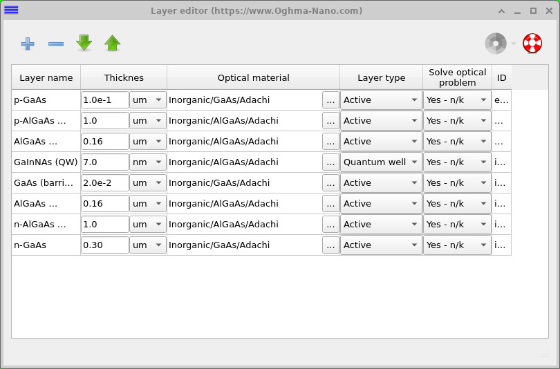
The layer editor (??) shows eight entries, running from p-GaAs through AlGaAs and the active region to n-GaAs. In particular, the central GaInNAs (QW) layer is 7.0 nm thick and its layer type is set to Quantum well. The visible example also includes 0.16 µm AlGaAs layers on either side of the active region and a 0.02 µm GaAs barrier/SCL layer. You do not need to reconstruct the stack manually when using the supplied template.
3.1 Inspecting the material definitions
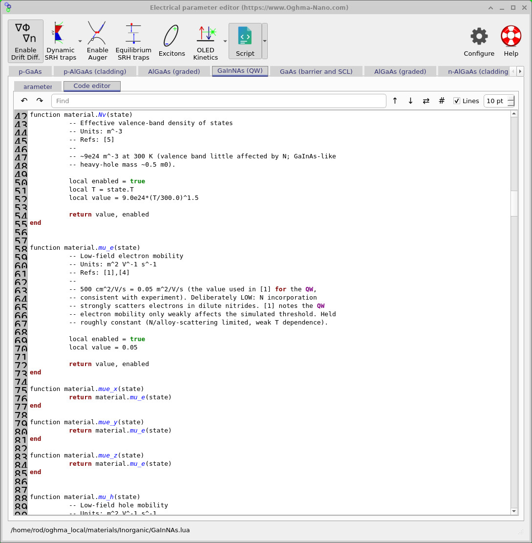
Click Electrical parameters, select the GaInNAs (QW)
tab and open Code editor
(??).
The screenshot illustrates how the material file contains physical quantities such
as the effective valence-band density of states and electrical mobility. For example,
the visible low-field electron mobility is 0.05 m² V⁻¹ s⁻¹, equivalent
to 500 cm² V⁻¹ s⁻¹. These are material-model inputs, not values inferred from the
plotted quantum-well dispersion.
In a dilute-nitride calculation it is especially important that composition, band-edge energies and nitrogen-coupling parameters are mutually consistent. For this first run, leave the template values unchanged; we will discuss a useful composition experiment at the end of the page.
4. What changes when we introduce nitrogen?
Before running the model, it is worth understanding why the Hamiltonian has ten bands rather than eight. Imagine the host semiconductor's conduction-band edge moving upwards in energy as the electron's in-plane wavevector increases. A nitrogen-related resonant state has its own characteristic energy. If the two states did not interact, their energies could approach and cross. In a dilute nitride, however, nitrogen couples to the host conduction states, changing the resulting energy levels.
A useful illustration of this physics is the two-state band-anticrossing (BAC) matrix:
\[ H_{\mathrm{BAC}}(k)= \begin{pmatrix} E_C(k) & V_N\\ V_N & E_N \end{pmatrix}, \qquad V_N=\beta_N\sqrt{x_N}. \]
Here, \(E_C(k)\) is the host conduction-band dispersion, \(E_N\) is the energy of the nitrogen-related level, \(x_N\) is the nitrogen fraction, and \(\beta_N\) controls the coupling strength. Diagonalising this small matrix gives two branches:
\[ E_{\pm}(k)=\frac{E_C(k)+E_N}{2} \pm\frac{1}{2}\sqrt{\big[E_C(k)-E_N\big]^2+4V_N^2}. \]
The square-root term prevents the coupled branches from crossing when \(V_N\neq0\). In particular, the lower conduction-like branch can move downwards relative to the original host conduction band, reducing the fundamental gap. Because the interaction depends on the separation between \(E_C(k)\) and \(E_N\), the dispersion can also become strongly non-parabolic.
This two-by-two example explains the central idea; it is not the complete quantum-well Hamiltonian solved in this tutorial. The ten-band k·p model retains the wider zincblende conduction/valence basis, including spin, and adds the nitrogen-related components. Quantum confinement is then included along the growth direction. For the complete theoretical treatment, see the ten-band zincblende chapter.
5. Running the simulation
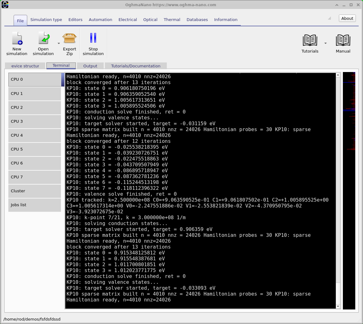
Return to the File ribbon and press Run simulation. Select the Terminal tab to follow the calculation (??). The solver assembles a sparse Hamiltonian, obtains the confined conduction and valence eigenstates, and repeats the calculation at a sequence of in-plane wavevectors \(k_{\parallel}\).
In the screenshot, the log identifies the KP10 solver, prints the calculated energy levels and reports block convergence after a number of iterations. The pairs of closely spaced energies can include spin-related degeneracies; they should not automatically be interpreted as distinct nitrogen-anticrossing branches. Wait for the run to finish before inspecting the output files.
6. Understanding the calculated band structure
The resulting plots show energy against in-plane wavevector, not energy as a function of depth through the device. The quantum-well potential confines carriers along the layer-growth direction, producing discrete states; motion parallel to the layers gives each confined state a dispersion \(E_n(k_{\parallel})\). In a simple parabolic model that dispersion is quadratic. A coupled ten-band Hamiltonian allows it to deviate from a parabola.
6.1 Conduction states and the reduced gap
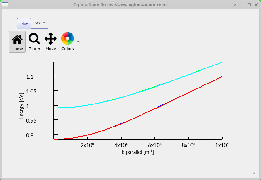
The conduction plot (??) shows two calculated branches starting at different energies. The lowest conduction state starts at approximately 0.89 eV in the chosen simulation energy reference. That number should not be confused with the bulk GaInNAs band gap: it is an eigenenergy of this particular confined structure. Notice that the two plotted curves do not have identical curvature. This is one feature to investigate when comparing an eight-band calculation against the dilute-nitride model.
The simplified BAC equations above help explain why the conduction dispersion can change in a nitrogen-containing material. They do not, on their own, prove the nitrogen weight of either coloured curve. That requires inspecting the corresponding eigenvectors or varying \(x_N\) and following how the states evolve.
6.2 Valence states
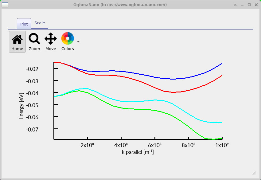
The valence plot (??) contains several branches with clearly non-parabolic shapes. Heavy-hole and light-hole character can mix at finite in-plane wavevector; the confinement energies, spin–orbit interaction and coupling between basis states all affect the curves. An upward turn or a change of curvature does not necessarily indicate a numerical failure. Conversely, a smoothly plotted curve is not by itself proof that the material parameters are correct.
Individual colours are best treated as plotted eigenstate branches, rather than permanently assigning HH or LH labels across the entire wavevector range without checking their state character.
6.3 Looking at both bands together
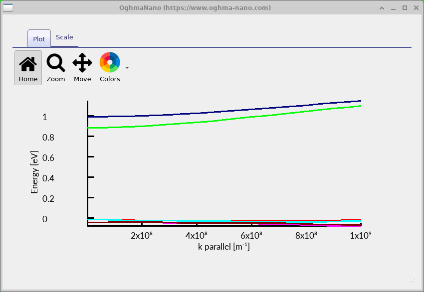
Opening the combined dispersion (??) places the electron and valence states on the same energy scale. The fundamental interband transition is related to their separation, rather than the absolute energy of either plotted state:
\[ \hbar\omega_{nm}(k_{\parallel}) =E_{c,n}(k_{\parallel})-E_{v,m}(k_{\parallel}). \]
This expression describes a direct, approximately vertical optical transition in the in-plane wavevector: photon momentum is small on the scale of the electronic crystal momentum. The observed spectrum is not generally one sharp line, however. Many allowed transitions contribute, with strengths and occupations that vary from state to state.
7. From electronic states to optical spectra
With the calculated states available, OghmaNano can construct optical spectra. The important physical question is not merely whether an electron and a hole have the right energy difference, but also how strongly the two states couple to the electromagnetic field and whether their initial and final states are occupied appropriately.
7.1 Why do some transitions contribute more than others?
Fermi's golden rule gives a useful starting point for understanding transition rates. For a transition from an initial electronic state \(i\) to a final state \(f\), induced by a weak optical perturbation, its schematic form is:
\[ W_{i\rightarrow f}=\frac{2\pi}{\hbar} \left|\langle f|H_{\mathrm{int}}|i\rangle\right|^2 \delta(E_f-E_i-\hbar\omega). \]
The matrix element \(\langle f|H_{\mathrm{int}}|i\rangle\) describes the interaction of the states with light. It depends, among other things, on their orbital character, envelope functions and light polarisation. The delta function enforces energy conservation. In a numerical spectrum, the idealised sharp transition is represented using an appropriate line-broadening function. After summing over allowed subbands and in-plane wavevectors, the result is a spectrum rather than a single transition energy.
Carrier occupations then distinguish absorption from emission. If \(f_c\) is the occupation of a conduction state and \(f_v\) the occupation of a valence electron state, the characteristic factors are:
\[ \begin{aligned} \text{absorption:}\quad &(1-f_c)f_v,\\ \text{stimulated emission:}\quad &f_c(1-f_v),\\ \text{net stimulated contribution:}\quad &f_c-f_v. \end{aligned} \]
The last expression is the difference between the upward and downward optical processes. A positive contribution to gain requires sufficient population inversion. These factors explain the interpretation of the following plots; see the optical transition theory for more detail.
7.2 Stimulated emission and absorption
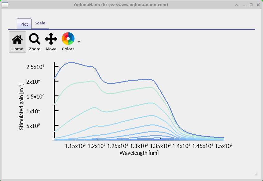
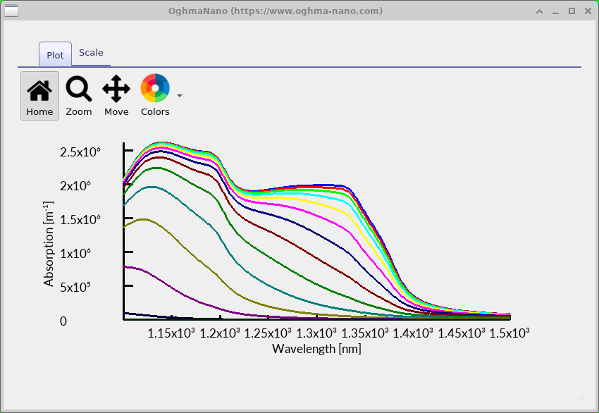
The two panels (?? and ??) illustrate competing optical processes for the same quantum-well band structure. Multiple curves represent the sequence of conditions used in the example; their relative magnitudes vary because the carrier occupations determine which transitions are available.
The spectra extend into the near infrared, broadly from about 1.1 to 1.5 µm. For orientation, photon energy and vacuum wavelength are related by:
\[ E_{\mathrm{photon}}=\frac{hc}{\lambda} \simeq \frac{1240\ \mathrm{eV\,nm}}{\lambda\,[\mathrm{nm}]}. \]
Thus, 1300 nm corresponds to approximately 0.954 eV. This provides a useful consistency check between the energy separation in the combined band plot and the scale of the optical spectra, bearing in mind confinement, the range of contributing transitions and the chosen energy reference.
7.3 Net gain: when emission overcomes absorption
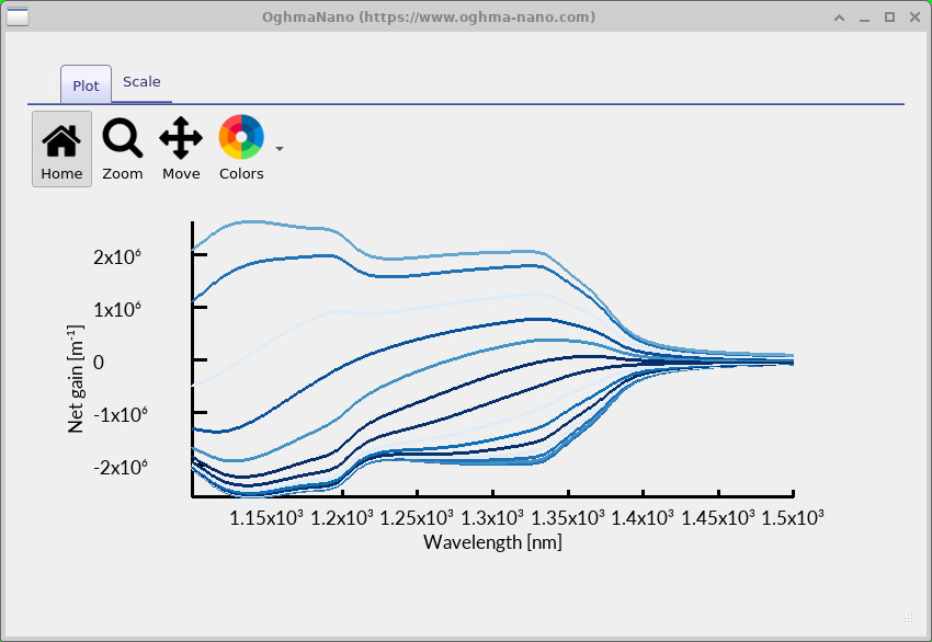
The quantity of interest for an amplifying medium is the balance between stimulated emission and absorption. With the sign convention used in the plot, it can be written schematically as:
\[ g_{\mathrm{net}}(\lambda) =g_{\mathrm{stim}}(\lambda)-\alpha(\lambda). \]
The calculated net-gain plot (??) includes both negative and positive curves. When absorption dominates, \(g_{\mathrm{net}}\) is negative. As the electron and hole populations change, stimulated emission may become strong enough for parts of the spectrum to develop positive material gain. The plotted transition region is notably structured, rather than being a perfectly smooth single peak, because multiple confined-state transitions contribute.
Important: positive material gain is not, by itself, a prediction that a complete laser will operate above threshold. Cavity losses, optical confinement, mirror reflectivity and carrier injection must also be considered.
8. Finding the simulation outputs
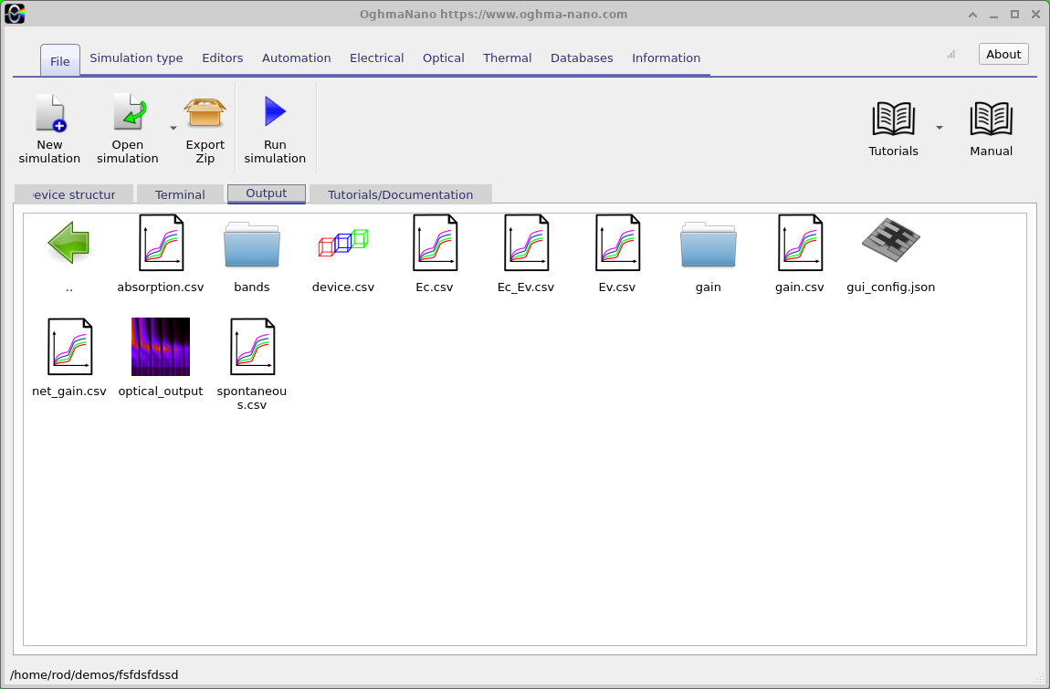
bands and gain subdirectories.
Once the calculation finishes, open the Output tab
(??).
The screenshot shows the main output files, including:
Ec.csv (conduction branches), Ev.csv (valence branches),
Ec_Ev.csv (combined bands), gain.csv,
absorption.csv, net_gain.csv and
spontaneous.csv. Additional results are organised within the
bands and gain directories. Double-click a CSV file
to plot it, or use the saved numerical data for further analysis.
Although this tutorial illustrates stimulated emission, absorption and net gain, the example also writes a spontaneous-emission output. Spontaneous emission is radiative recombination without the need for an incoming photon, and its characteristic occupation factor is \(f_c(1-f_v)\). Its absolute spectral prefactors differ from those of stimulated emission.
9. Try it yourself: investigate the nitrogen interaction
Suggested experiment: Save a separate copy of this working example before editing it. Then investigate the nitrogen concentration in the GaInNAs material definition, changing one parameter at a time while keeping the 7 nm well geometry fixed.
- Record the lowest electron eigenenergy at \(k_{\parallel}=0\).
- Change the nitrogen fraction within a physically appropriate range for the selected parameterisation.
- Recalculate the conduction dispersion and compare the shape of the lowest branch.
- Compare the position of the absorption edge and the main gain features.
The BAC illustration predicts that increasing the nitrogen coupling can increase the separation of the coupled branches and alter the lower conduction energy. In a complete alloy calculation, however, composition may affect other material parameters too. Therefore, interpret any resulting changes using the actual material functions enabled in your simulation rather than assuming the simple two-state formula is the full alloy model.
✅ What to look for
Investigate whether the conduction-band edge moves and whether its curvature changes as nitrogen concentration is varied. Compare the optical spectra at identical occupation settings, so that a change in the transition energies is not confused with an unrelated change in carrier population. If you can inspect eigenvector composition, it is particularly informative to follow the changing host-conduction and nitrogen-related contributions to the states.
For a second experiment, keep the material parameters fixed and change the quantum-well width from 7 nm to 6 nm. Increasing quantum confinement generally pushes the lowest confined electron energy upwards and changes the allowed interband transition energies. The magnitude of the shift is determined by the coupled ten-band calculation, not simply by assigning a single constant effective mass to every state.
📘 Continue with the ten-band dilute-nitride k·p theory for the full electronic model, or see optical transitions and matrix elements for a fuller treatment of the physics behind these spectra.