What are perovskite semiconductors? Materials, devices and applications
1. What are perovskite semiconductors?
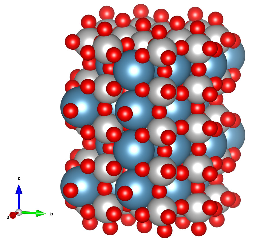
Perovskite semiconductors are a class of crystalline materials defined by their ABX\(_3\) crystal structure, where A and B are cations and X is an anion. In optoelectronic applications, the most widely studied materials are hybrid organic–inorganic lead halide perovskites. These materials combine strong optical absorption, long carrier diffusion lengths and relatively simple fabrication routes (see ??).
Unlike organic semiconductors, perovskites are crystalline and can often be described using band transport. However, they do not behave like conventional silicon or III–V semiconductors. Their device physics is strongly influenced by defects, interfaces and slow internal processes, making them a distinct class of thin-film semiconductor.
2. Key physical properties of perovskite semiconductors
Perovskite materials exhibit a combination of properties that are unusual in semiconductor physics. They typically show strong absorption coefficients, allowing thin films to absorb most incident light. Charge carriers can travel relatively long distances before recombining, which is why high-efficiency devices can be achieved even in comparatively thin layers.
At the same time, perovskites are defect tolerant. Many defects introduce shallow states rather than deep recombination centres, which allows good performance despite imperfect material quality. However, this does not mean defects are unimportant. Interfaces, grain boundaries and trap states can still dominate recombination and device behaviour under operating conditions.
A defining feature of many perovskite materials is the presence of mobile ionic species. Ions can migrate under electric fields, altering the internal electrostatic potential over time. This leads to phenomena such as hysteresis, time-dependent response and measurement-history dependence. A detailed treatment is given in perovskite ion physics.
3. Perovskite device physics
The behaviour of a perovskite device is not determined by a single mechanism. Instead, it emerges from the interaction of optical generation, charge transport, recombination, defect states, interfaces and ionic motion. These processes occur on different timescales and are strongly coupled.
For example, ionic motion can redistribute internal electric fields, which in turn changes carrier extraction and recombination rates. Similarly, trap occupation affects carrier lifetimes, which influences both steady-state and transient behaviour. As a result, measured quantities such as JV curves or transient responses reflect a coupled system rather than a simple transport problem.
4. Perovskite electronic devices
The most prominent application of perovskite semiconductors is in photovoltaics, but the same materials platform is also being explored for other optoelectronic devices.
- Perovskite solar cells convert absorbed light into electrical current. Their performance depends on optical absorption, carrier transport, recombination and contact selectivity. See the perovskite solar cell simulation tutorial.
- Perovskite light-emitting devices use radiative recombination to produce light. These devices depend strongly on recombination pathways, defect states and optical outcoupling.
- Perovskite photodetectors exploit strong absorption and long carrier lifetimes to detect light across a range of wavelengths.
5. Advantages of perovskite semiconductors
Perovskites are attractive because they combine high performance with relatively simple fabrication. Thin films can often be deposited at low temperature using solution-based or vapor-based techniques. Their strong absorption allows efficient devices with relatively thin layers, reducing material usage.
In photovoltaics, this combination has enabled rapid increases in efficiency over a short period of time. Perovskites are also compatible with tandem architectures, where they are combined with silicon or other materials to exceed the efficiency limits of single-junction devices.
6. Limitations and challenges
Despite their advantages, perovskites face several challenges. Stability remains a major issue, with degradation under heat, moisture, oxygen and illumination. Ion migration introduces time-dependent behaviour that complicates both measurement and modelling.
Interfaces are also critical. Recombination at contacts, interfacial trap states and imperfect band alignment can dominate device performance. This means that high device efficiency requires careful control not only of the active material but also of the full device stack.
7. Why modelling perovskites is different
Perovskite device simulation requires a coupled treatment of electronic and ionic processes. A standard drift–diffusion framework is used to describe carrier transport and recombination, but this must be extended to include trap states, interfacial effects and mobile ions.
Recombination is often described using Shockley–Read–Hall (SRH) theory, while ionic motion modifies the electrostatic potential over time. This coupling between transport, recombination and ionic redistribution is what gives rise to hysteresis and time-dependent device behaviour.
8. Where perovskites may win
Perovskites are already competitive in photovoltaics, particularly in research-scale devices and tandem architectures. Their ability to be processed at low temperature and integrated with other materials makes them attractive for next-generation solar technologies.
However, they are unlikely to replace silicon in all applications. Long-term stability, scalability and manufacturing reliability remain key challenges. Their most likely role is as part of hybrid systems, where their strengths complement those of more established semiconductor technologies.
9. Simulating perovskites in OghmaNano
OghmaNano provides a simulation environment for modelling perovskite devices as coupled optical, electrical and ionic systems. It includes drift–diffusion transport, recombination models, optical generation and mobile ion dynamics in a unified framework.
For practical examples, see the perovskite device modelling overview, which links to tutorials covering JV curves, EQE, CELIV and large-area modules.