Perovskite solar cell simulation: JV, EQE, CELIV and modules
1. Introduction to perovskite semiconductors
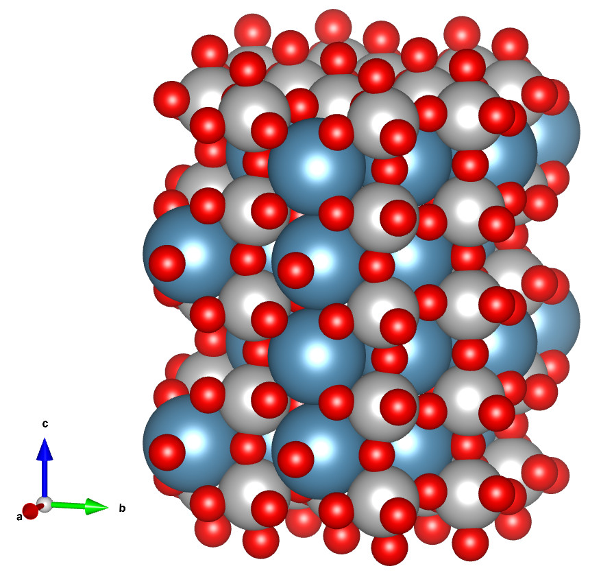
Perovskite semiconductors are crystalline thin-film materials with strong optical absorption, long carrier diffusion lengths and relatively low-cost fabrication. Unlike disordered organic semiconductors, carriers in perovskites can often be described using band transport, but the device behaviour is still strongly influenced by defects, interfaces and slow internal processes (see ??). A detailed discussion of ionic effects and internal dynamics can be found in perovskite ion physics.
The key challenge in perovskite device simulation is that multiple physical processes occur on very different timescales. Fast electronic transport and recombination coexist with slower processes such as trap occupation, interfacial charge accumulation and ion migration. These slow processes can modify the internal electric field, leading to hysteresis, time-dependent behaviour and measurement-dependent device response.
As a result, the measured current–voltage curve is not a simple steady-state characteristic, but a coupled outcome of optical generation, carrier transport, recombination, contact selectivity and internal field redistribution. Transient methods (such as CELIV) and intensity-dependent measurements (such as Suns-Voc and Suns-Jsc) are therefore often required to fully understand device behaviour.
In OghmaNano, perovskite devices are modelled using a drift–diffusion framework that couples charge transport, recombination, optical generation and mobile ion redistribution. This allows simulations to connect directly to experimental observables such as JV curves, EQE, transient extraction signals, hysteresis and light-intensity-dependent behaviour, providing a physically consistent interpretation of device performance.
2. Perovskite solar cell tutorials
The basic perovskite solar cell tutorial is the recommended starting point. It introduces the device stack, runs a standard simulation and shows how the electrical output can be interpreted. Once this workflow is understood, the same model can be extended to spectral response, charge-extraction and light-intensity-dependent measurements.
- Perovskite solar cell simulation — build a perovskite photovoltaic device simulation, calculate a JV curve, and interpret \(J_{SC}\), \(V_{OC}\), fill factor and efficiency in terms of generation, recombination, transport and extraction.
3. Perovskite transient and charge-extraction methods
Transient measurements are useful because they probe how charge is stored, transported and extracted from the device. In perovskite solar cells, this can be especially important because slow internal processes may influence the apparent electrical response. A transient simulation can therefore reveal information that is hidden in a steady-state JV curve.
- Perovskite solar cell CELIV example — simulate charge extraction by linearly increasing voltage, and study how extracted current transients depend on carrier density, mobility, recombination and internal electric field.
4. Spectral response and illumination-dependent measurements
Perovskite devices are commonly characterised using EQE and light-intensity-dependent measurements. These simulations are valuable because they separate different parts of the device response. EQE connects wavelength-dependent optical absorption to collected current, while Suns-Voc and Suns-Jsc probe how voltage and current respond as the illumination intensity changes.
These measurements are especially useful when a single JV curve is not enough. A device can show similar power-conversion efficiency for different physical reasons: stronger absorption, better transport, lower recombination, improved contact selectivity or reduced series resistance. Spectral and light-intensity-dependent simulations help distinguish between these possibilities.
- Perovskite solar cell EQE example — calculate wavelength-dependent external quantum efficiency and connect optical absorption, carrier generation and charge collection to the measured spectral response.
- Perovskite Suns-Voc example — simulate open-circuit voltage as a function of light intensity, useful for studying recombination, ideality-factor-like behaviour and voltage losses.
- Perovskite Suns-Jsc example — simulate short-circuit current as a function of light intensity, useful for studying generation, collection, transport limitations and photocurrent linearity.
5. Large-area perovskite devices
Small-area perovskite cells are useful for understanding material and interface behaviour, but module-scale devices introduce additional physics. Series resistance, contact geometry, lateral current flow, non-uniform illumination and layout-dependent losses can all become important when scaling from a lab cell to a larger device.
- Large area perovskite module — simulate a larger-area perovskite module and study how scaling, geometry and resistance influence the electrical output of the device.
6. Underlying physics
The perovskite tutorials above are built on OghmaNano’s semiconductor device-modelling framework. The central electrical model is drift–diffusion transport coupled to Poisson’s equation, optical generation and recombination. In practical terms, this means the simulation solves how carrier density, electrostatic potential, current flow and recombination vary through the device under bias and illumination.
This is important because perovskite solar cell performance is rarely controlled by a single parameter. A change in mobility, defect density, contact selectivity, layer thickness or optical absorption can change the internal carrier distribution; that changes recombination and field redistribution; and that in turn changes the measured JV curve, EQE or transient response.
- Theory of drift–diffusion modelling — the electrical transport framework used to solve carrier continuity, current flow and electrostatic coupling in device simulations.
- Shockley–Read–Hall recombination — trap-assisted recombination and defect-mediated carrier loss, often central to thin-film semiconductor device performance.
- Non-equilibrium SRH trapping and recombination — numerical treatment of trapping, emission and recombination where equilibrium assumptions are not sufficient.
- Charge carrier mobility — mobility models, transport assumptions and interpretation of mobility in semiconductor device simulations.
- Wave optics, FDTD, mode solvers & TMM — optical simulation tools for thin-film stacks, guided modes and full-field electromagnetic simulations.
8. Where should you start?
If you are new to OghmaNano, start with the basic perovskite solar cell simulation tutorial. It gives the fastest route to a working device simulation: define the stack, run the model, inspect the JV curve and connect the result to physical quantities such as generation, extraction, recombination and voltage loss.
If you already understand the basic workflow, move into the measurement-specific tutorials. Use CELIV for transient charge extraction, EQE for spectral response, Suns-Voc and Suns-Jsc for light-intensity-dependent behaviour, and the module tutorial when scaling effects become important.