

2D FDTD Perovskite Solar Cell Tutorial: Coupled FDTD and Drift-Diffusion Simulation
1. Introduction
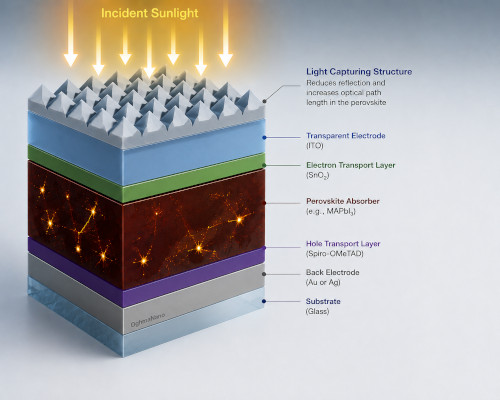
This tutorial demonstrates a coupled 2D finite-difference time-domain (FDTD) and drift-diffusion simulation of a textured perovskite solar cell. The FDTD solver calculates the optical field and absorption inside the device. The resulting spatial carrier-generation rate is passed directly to the electrical solver, which calculates transport, recombination, charge extraction, and the final current density–voltage (JV) curve.
The device includes a light-trapping surface structure, shown in ??. This structure reduces front-surface reflection, redirects light into oblique paths, and increases the optical path length through the perovskite absorber. It can therefore improve absorption without increasing the absorber thickness, which may otherwise increase recombination and reduce carrier collection.
A one-dimensional optical model such as the transfer matrix method is suitable for flat, laterally uniform layer stacks. It cannot fully describe lateral scattering from a textured surface. In this device, the optical field varies both across the cell and through its thickness, so a 2D FDTD model is used to solve Maxwell’s equations on a spatial grid.
FDTD provides the local electric field \(\mathbf{E}(x,y)\). From this, OghmaNano calculates the absorbed optical power density and converts it into the spatial optical generation rate \(G(x,y)\), in \(\mathrm{m^{-3}\,s^{-1}}\). The drift-diffusion solver then uses \(G(x,y)\) to calculate carrier densities, electrostatic potential, recombination, current flow, and quasi-Fermi levels as the voltage is swept.
This coupled approach is important because increased optical absorption does not always produce an equivalent increase in photocurrent. Carriers generated in regions with strong recombination or poor transport may not be collected efficiently. The simulation therefore evaluates the light-trapping structure in terms of the final electrical output, rather than absorption alone.
In this tutorial, you will run the complete optoelectronic simulation, inspect the device mesh and optical generation profile, examine the electrical carrier distributions, and compare the JV curves with and without the light-trapping structure.
2. Making a new simulation
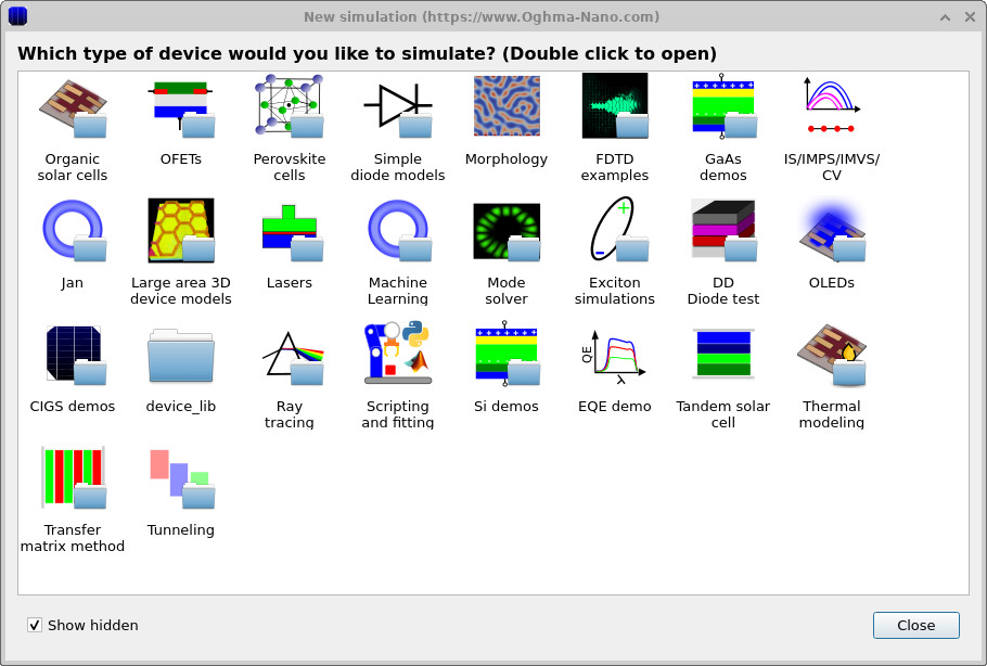
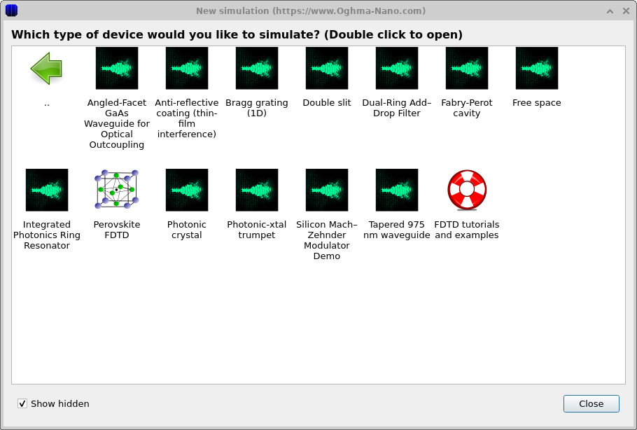
Open the New simulation window and select the FDTD examples category (??). Then choose the Perovskite FDTD example (??). Save the simulation to a suitable folder; this loads the main interface shown in ??.
3. Orienting yourself in the main window
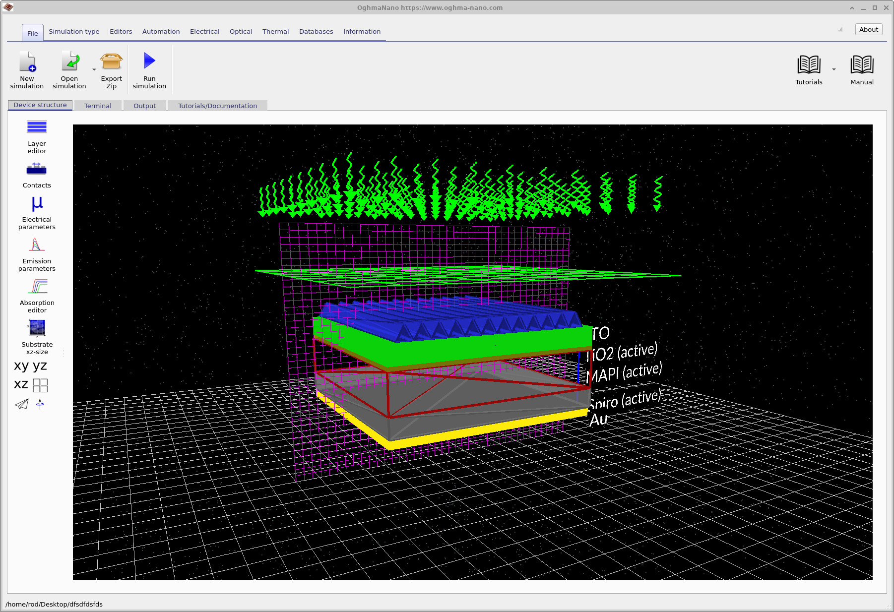
After loading the simulation, the main window will appear as shown in ??. The structure is displayed in the 3D view in the Device structure tab. The black background represents the world - the simulation domain in which the device sits.
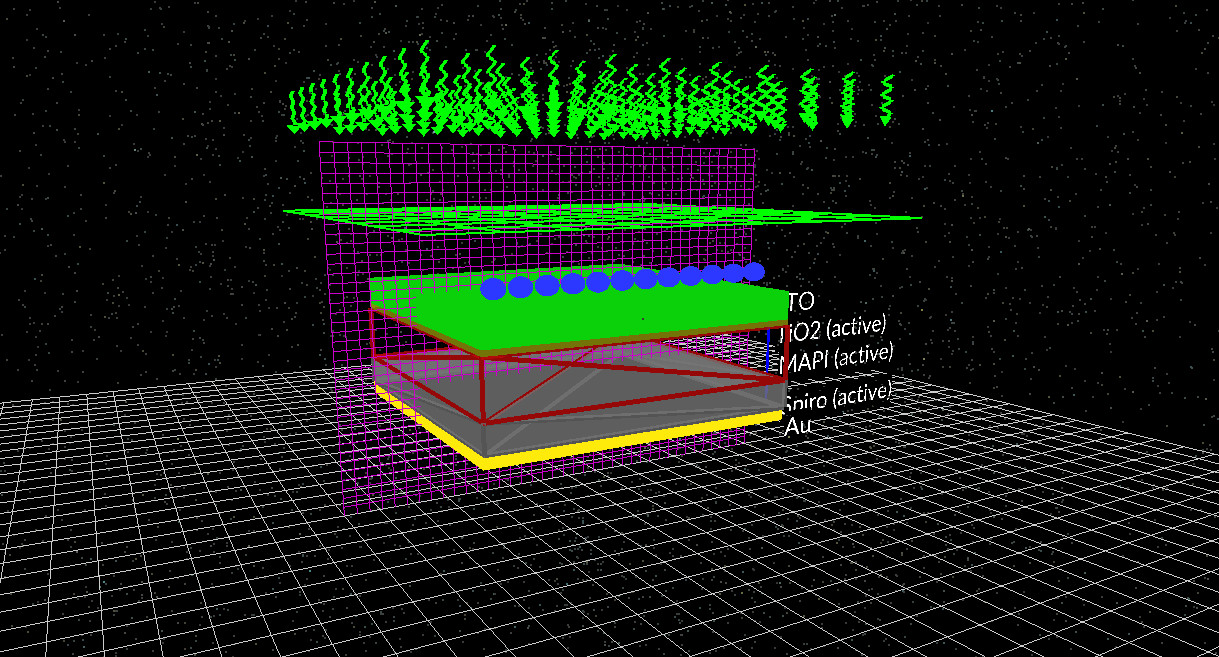
Several important elements are visible. At the top of the device, the block of green arrows represents the FDTD light source. Light is injected from above and travels downwards into the cell, just as sunlight would illuminate a real solar cell. Below the source you can see a detector plane: this measures the electromagnetic field as light passes through it, and its readings are essential for later reconstructing the optical generation profile inside the device.
Running vertically through the structure is a purple grid. This is the FDTD mesh, and it shows the plane through which the simulation is solved - in effect we are taking a 2D slice through the device. Near the top of the cell you can also see a triangular light-trapping structure, which is designed to scatter incoming light and increase absorption. Beneath it lie the functional perovskite device layers (for example the transparent contact, electron and hole transport layers, the perovskite absorber, and the metal back contact) stacked to form the working solar cell.
It should be noted that the detectors do not interfere with the light itself; they simply measure the electromagnetic fields.
In a moment we will run the simulation and watch how light travels down into the structure, is scattered by the light-trapping layer, and is absorbed in the perovskite. This absorption is what generates the charge carriers that the electrical model subsequently collects.
4. Running the simulation
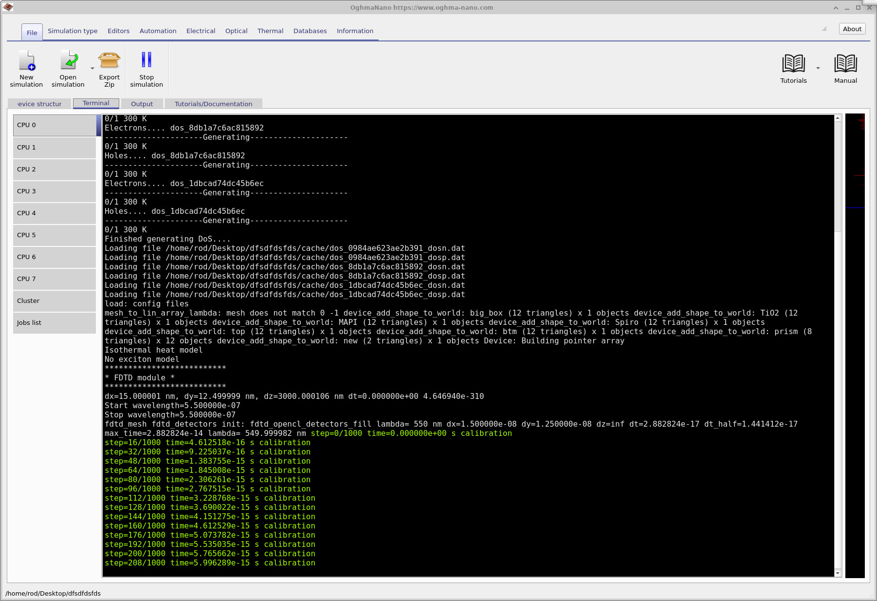
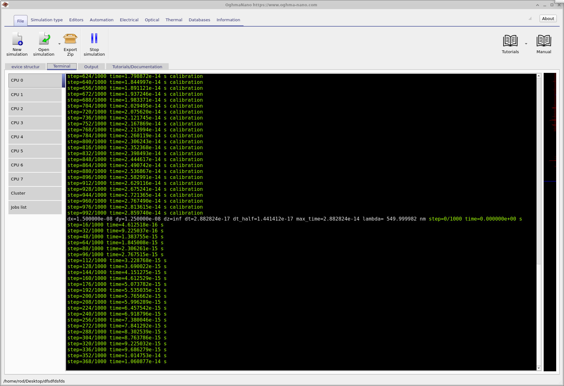
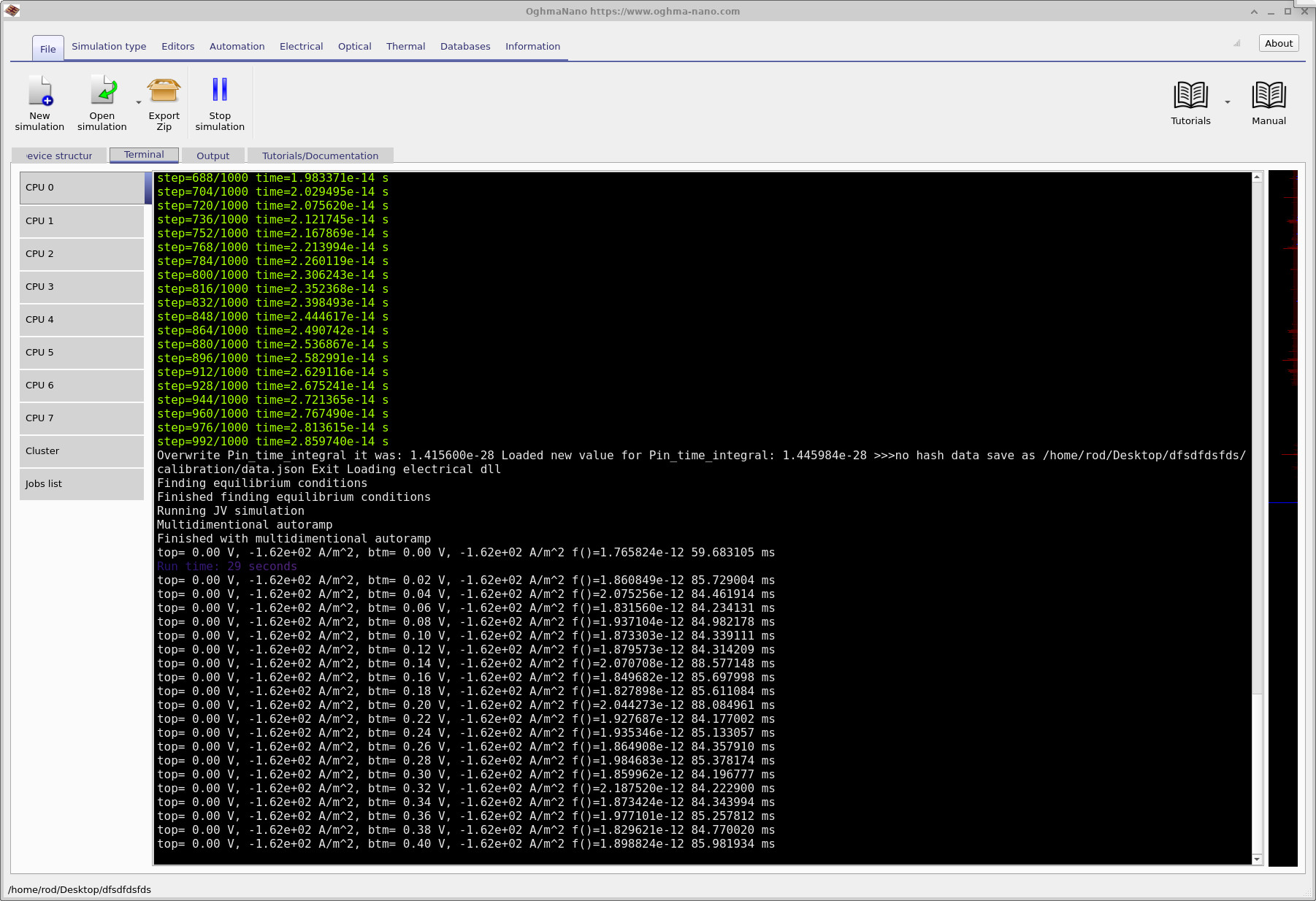
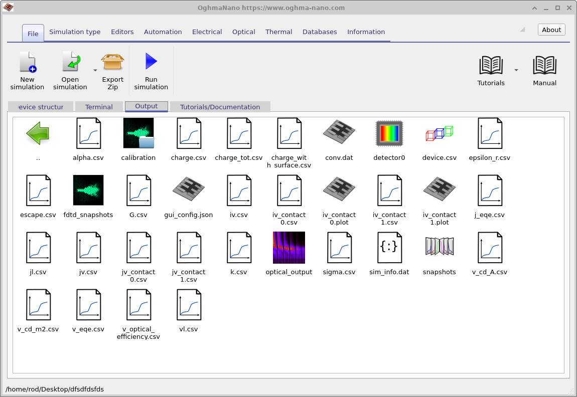
Once you have saved the simulation and had a look around the structure, click the Run simulation (▶) button to start the calculation. The window will switch to the Terminal tab, where you can follow the progress of the run. The simulation proceeds through several stages, shown in ??–??, and produces the outputs shown in ??.
Calibration run.
As the FDTD module starts (??),
the very first thing it does is a calibration simulation. In this step OghmaNano temporarily removes the device
from the domain and propagates the source pulse through empty space. This records a clean reference measurement of
the incident field at the detectors - how much light would arrive if the device were not there at all. Later, the code compares
the real run (with the device present) against this reference. That comparison is what allows OghmaNano to separate the light that
is reflected, transmitted, and genuinely absorbed, and therefore to calculate the optical generation profile inside the cell
accurately. While calibration is running, each printed line is tagged with the word calibration.
Main optical run.
Once calibration is complete (??),
the word calibration disappears from the output and the real FDTD simulation of the device begins, stepping the
electromagnetic field forward in time. Notice that the progress text is printed in green. This is deliberate: this
particular example is solved at a single wavelength of roughly 550 nm, which lies in the green part of the
visible spectrum, and OghmaNano colours the timestep text to match the wavelength currently being simulated.
Electrical run. When the FDTD stage finishes, the terminal reports the elapsed time - here the optical run took around 30 seconds (??). It is worth noting that FDTD is inherently slow, because it explicitly simulates the propagation of light through the structure timestep by timestep. Once the optics are done, OghmaNano automatically moves on to the electrical simulation and sweeps out a JV curve using the generation profile that FDTD has just calculated. In the terminal you will see the applied voltage stepped from 0 V upwards, together with the resulting current density. A negative current density indicates that the cell is generating current - i.e. it is behaving as a working solar cell under illumination.
When the run has completed, switch to the Output tab (??) to find the data generated during the simulation. We will look at the most important outputs in the next section.
5. Viewing the results
With the run complete, we can inspect the outputs from the Output tab (??). We will focus on the three most informative results: the device mesh, the optical generation profile, and the JV curve.
Device mesh.
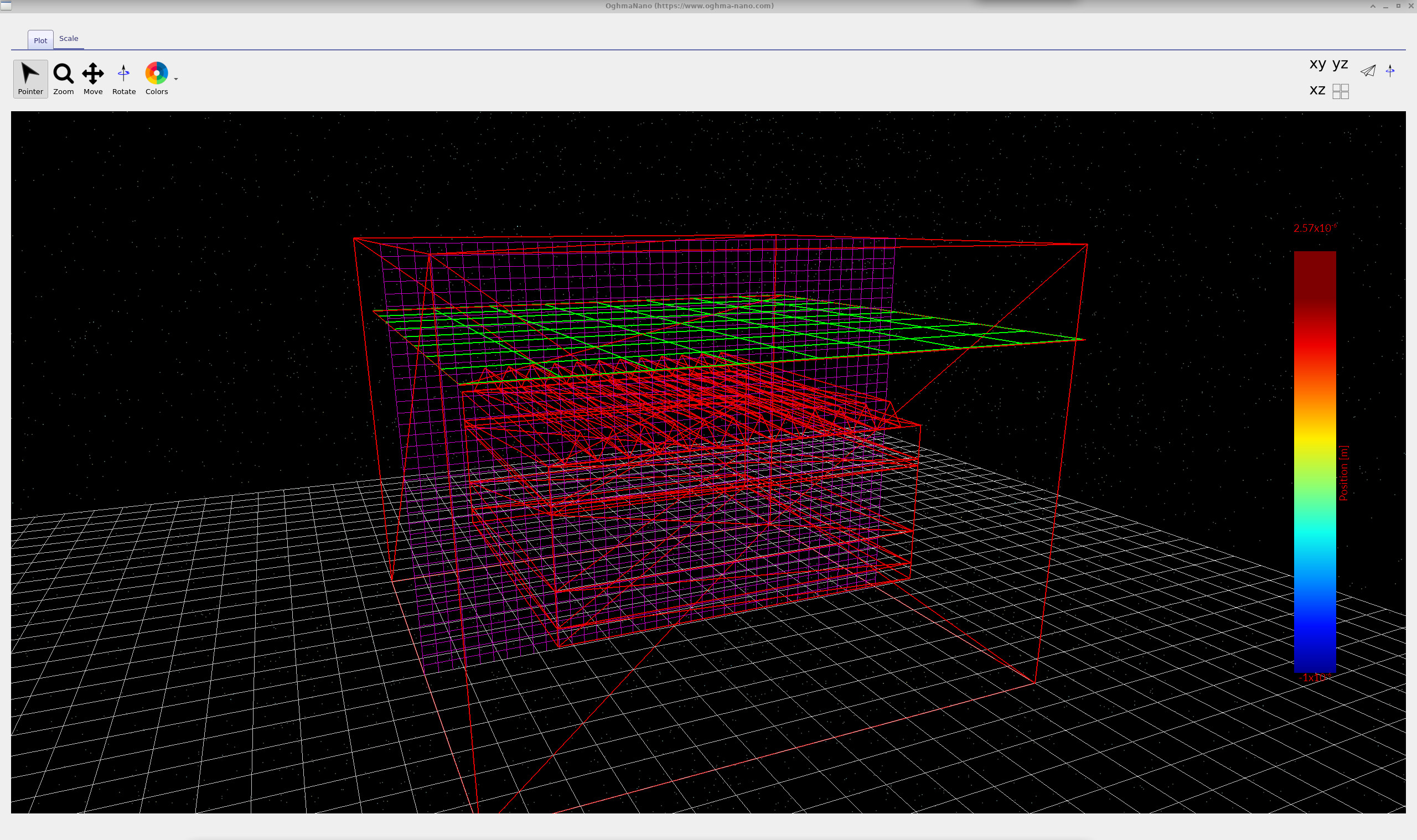
First, open device to view the geometry, shown in
??. This reveals how OghmaNano
actually represents the structure internally: the entire device is discretised into a large number of triangles.
This triangular mesh is what the solver really “sees”, and you can rotate and zoom around it freely to inspect how the
layers and the light-trapping structure are built up.
Optical generation profile.
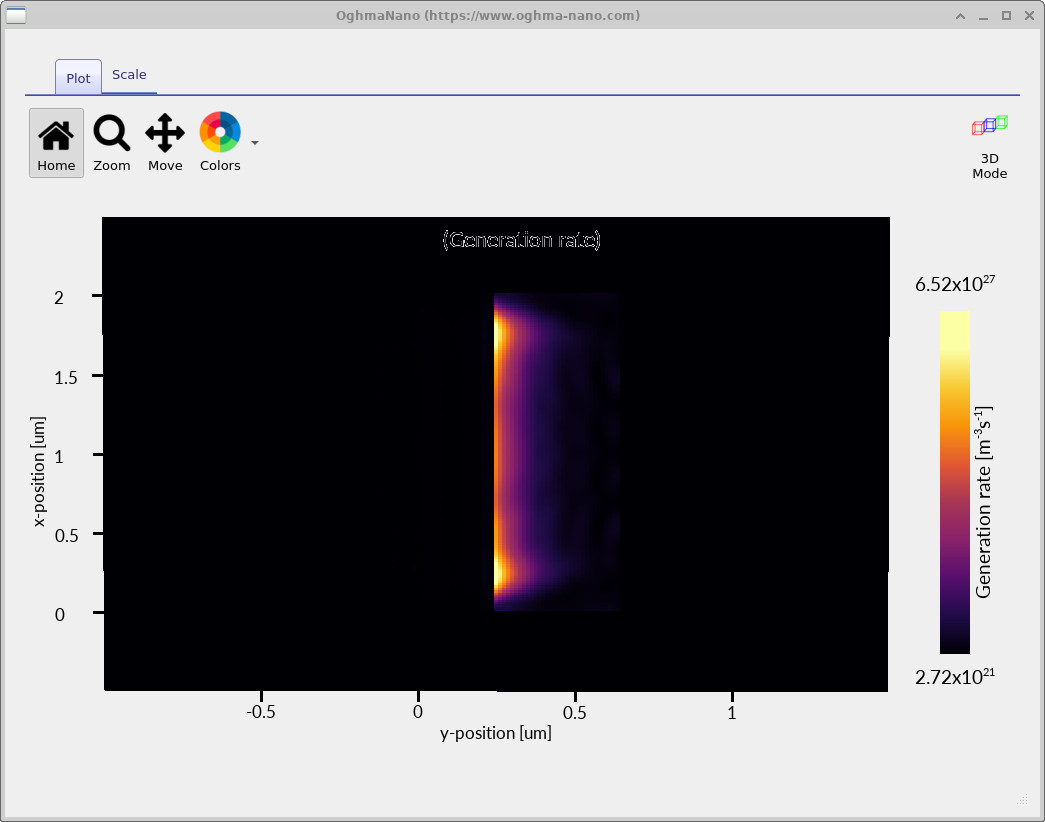
Next, open G to view the optical generation rate, shown in
??. This is the spatial map of
where electron–hole pairs are created inside the device, calculated directly from the FDTD field. It is plotted in units of
\(\mathrm{m^{-3}\,s^{-1}}\), i.e. the number of carriers generated per unit volume per second. You can clearly see the generation
concentrated within the active region, with brighter regions where the light-trapping structure has enhanced absorption. This
profile is precisely the quantity that is passed to the electrical model.
JV curve.
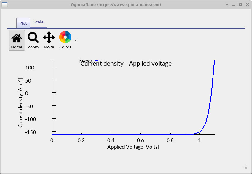
Finally, and most importantly for a quick assessment of device performance, open jv to view the
current density–voltage curve, shown in
??. For this example the cell reaches an
open-circuit voltage (\(V_{oc}\)) of just over 1 V and a short-circuit current density (\(J_{sc}\)) of
roughly −150 A m−2. The negative sign simply reflects the sign convention that
photogenerated current flows in the opposite direction to an applied forward bias. Note that, as everywhere in OghmaNano, all
quantities are expressed in SI units.
6. Examining the results in detail
The simulation we have just run really has two parts: an FDTD optical calculation and a drift-diffusion electrical calculation. OghmaNano saves detailed snapshots from both stages, and we can step through them to understand exactly what is happening inside the device. We will look at the optical results first and then the electrical results.
The FDTD (optical) snapshots.
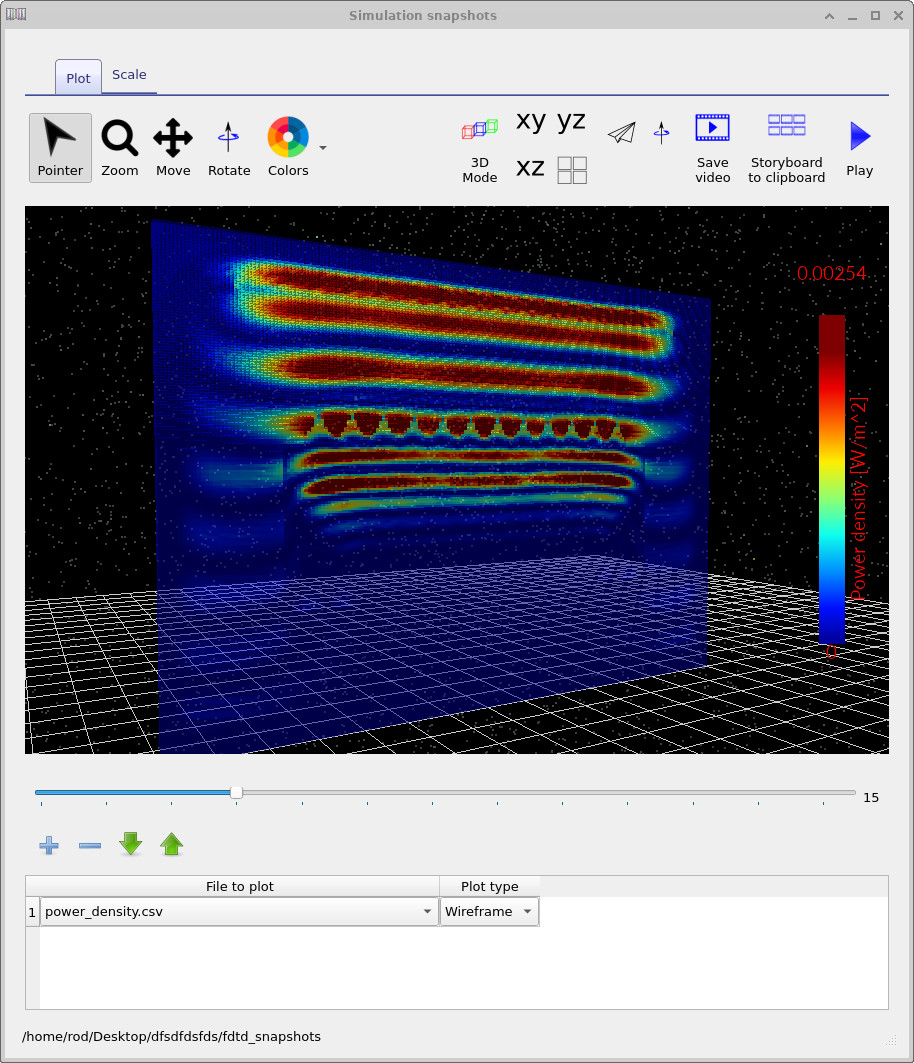
From the Output tab, double-click on fdtd_snapshots. This opens the snapshot viewer shown in
??, which is essentially a
complete dump of the FDTD field as it evolved during the run. The viewer lets you inspect the results as a function of simulation
step. Click the blue + button and select power_density.csv, then drag the scroll bar to move through
the timesteps and watch how the field propagates down into the device and is scattered by the structure. If you would rather look
at the raw field components, you can add Ex, Ey, or Ez instead of the power density.
The electrical snapshots.
The electrical results are stored separately. From the Output tab, double-click on the snapshots directory
(as opposed to fdtd_snapshots). Using the + button, add Ec.csv, Ev.csv,
Fn.csv, and Fp.csv to plot the conduction band edge, the valence band edge, and the electron and hole
quasi-Fermi levels, as shown in
??. Note that
this time the slider steps through applied voltage rather than time (the window title reports the current bias,
e.g. 0.1 V), so you can watch the band structure respond as the cell is swept from short circuit towards open circuit.
Carrier densities.
A closely related view is obtained by adding Q_nfree.csv and Q_pfree.csv, which give the free electron
and free hole densities (in \(\mathrm{m^{-3}}\)). The result is shown in
??. Again, stepping the
slider through voltage lets you see how the electron and hole populations redistribute across the device as the applied bias
changes.
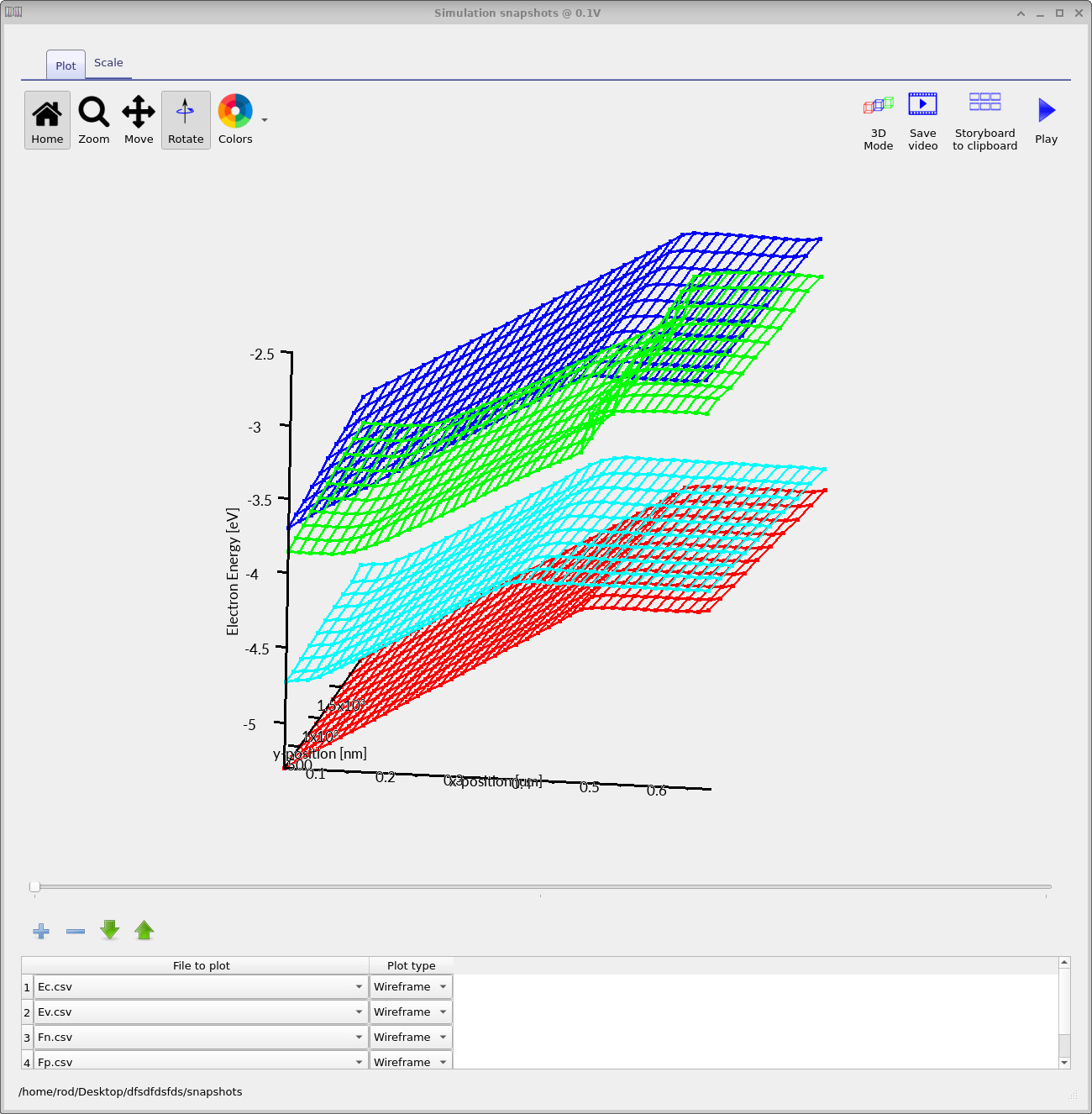
Ec, Ev) and quasi-Fermi levels (Fn, Fp), stepped through voltage.
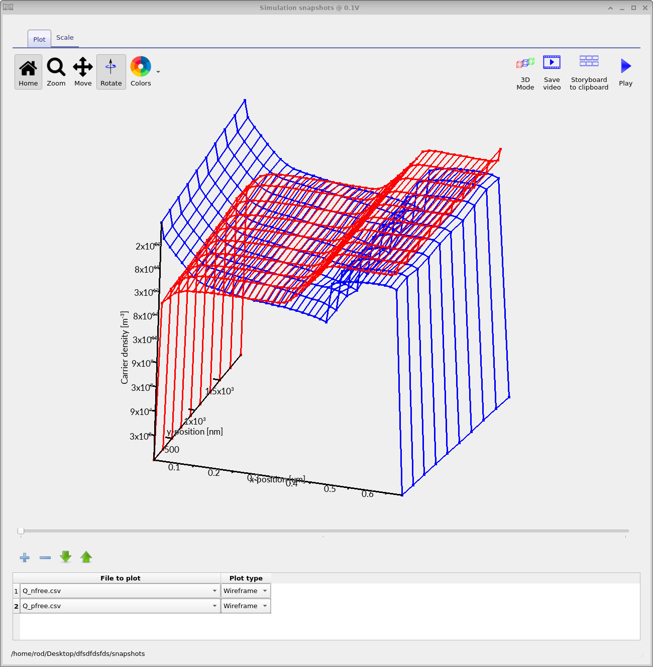
Q_nfree) and free holes (Q_pfree) as a function of voltage.
7. The effect of the light-trapping structure
The triangular layer on top of the cell is a textured light-trapping structure (it also acts as an anti-reflection layer). We can use the simulation to measure exactly what it does by switching it off and comparing the result against the original device.
Save a reference JV curve.
Before changing anything, make a copy of the results file jv.csv and rename the copy jv_backup.csv using
your operating system’s file manager. This preserves the JV curve of the full device so that we can compare against it later.
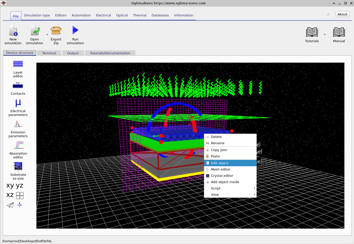
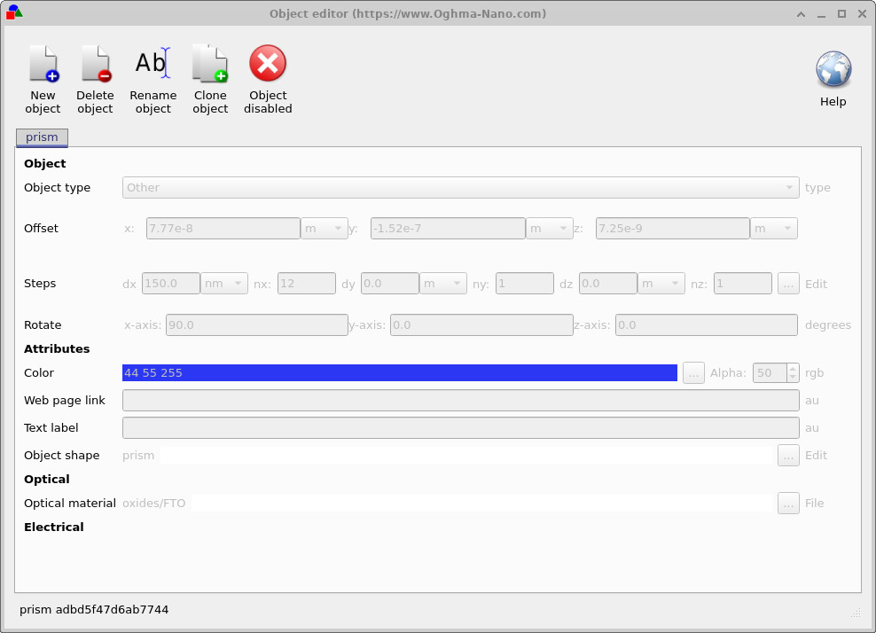
Disable the structure. Right-click on the triangular structure on top of the device and select Edit object, as shown in ??. This opens the object editor, shown in ??. Click the enable/disable button in the toolbar so that it reads Object disabled. The triangular structure will now disappear from the device, leaving the flat stack shown in ??.
What have we actually removed? A textured layer like this does two useful things for a solar cell. First, by replacing the abrupt flat interface with a graded, angled surface, it reduces front-surface reflection, so more light enters the device instead of bouncing straight back off the top. Second, it scatters and redirects the transmitted light so that it travels at an angle and follows a longer path through the absorber, increasing the chance of absorption. Together these effects raise the total absorbed light and therefore the short-circuit current. In real devices - silicon cells are the classic example, where micron-scale pyramids are routinely etched into the surface - this benefit is well established but can be difficult to isolate and quantify experimentally. A simulation lets us switch the structure on and off and read off its effect directly.
Rerun and compare.
With the triangular structure now disabled, rerun the simulation. This produces a fresh jv.csv for
the device without the light-trapping layer. Plot this new jv.csv together with the saved jv_backup.csv
(the full device) on the same axes; you should obtain something like
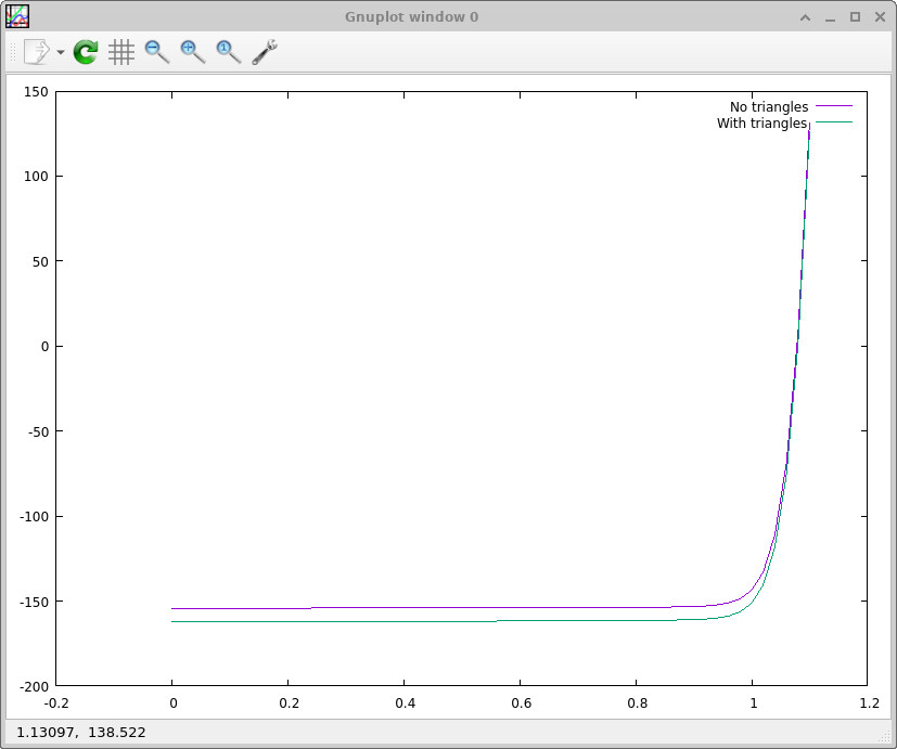
??. The difference is modest but
clearly visible: with the light-trapping structure in place, the magnitude of the short-circuit current is larger (around
−162 A m−2) than without it (around −155 A m−2). This confirms
that the texture increases the amount of light absorbed and hence the current the cell can deliver.
8. Reducing the dimensionality of the electrical problem
A full multidimensional simulation is not always necessary. In many layered solar cells, the dominant variation is through the device thickness, so a well-resolved 1D model can reproduce the important physics at a fraction of the computational cost. Higher-dimensional models are most useful when the device geometry or the transport itself varies laterally.
In this example, the textured light-trapping surface makes the optical problem genuinely two-dimensional. Light is scattered sideways, so the optical field varies in both the x direction and through the device thickness. The electrical problem is different: charge transport is still dominated by motion through the layer stack, so a 1D drift-diffusion model may be sufficient.
This distinction is important because a coupled 2D FDTD and 2D drift-diffusion simulation is considerably more expensive than a reduced model. We will therefore keep the optical calculation in 2D, where the texture matters, and test whether the electrical calculation can be reduced to 1D without losing the behaviour of interest.
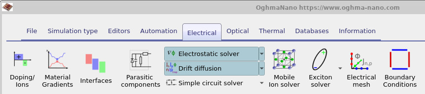
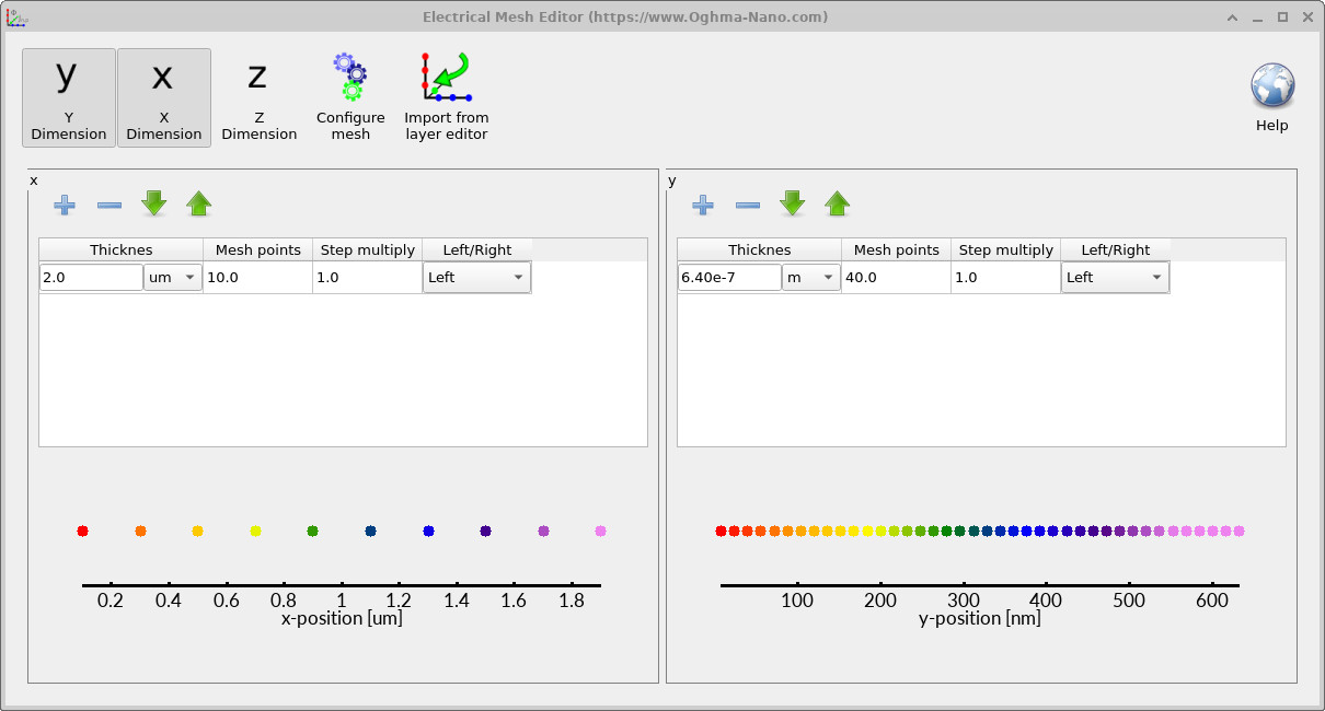
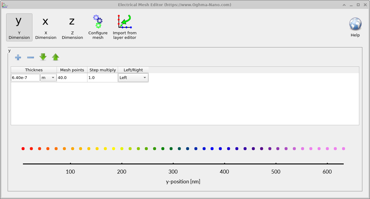
Open the Electrical ribbon, shown in ??, and click Electrical mesh. The mesh editor is shown in ??. The device is discretised using 40 points in the y direction, through the layer stack, and 10 points in the lateral x direction. The finer y mesh resolves the band bending, carrier gradients, recombination, and current flow through the device.
To reduce the electrical model to one dimension, click X Dimension at the top of the mesh editor. This removes the lateral x mesh and leaves only the through-thickness y mesh, as shown in ??. The optical simulation remains 2D, but the drift-diffusion calculation is now a faster 1D electrical model.
Rerun the simulation. The model now uses a 2D optical simulation coupled to a 1D electrical simulation. The FDTD solver still resolves the lateral scattering caused by the light-trapping structure, while the drift-diffusion solver treats carrier transport only through the device thickness.
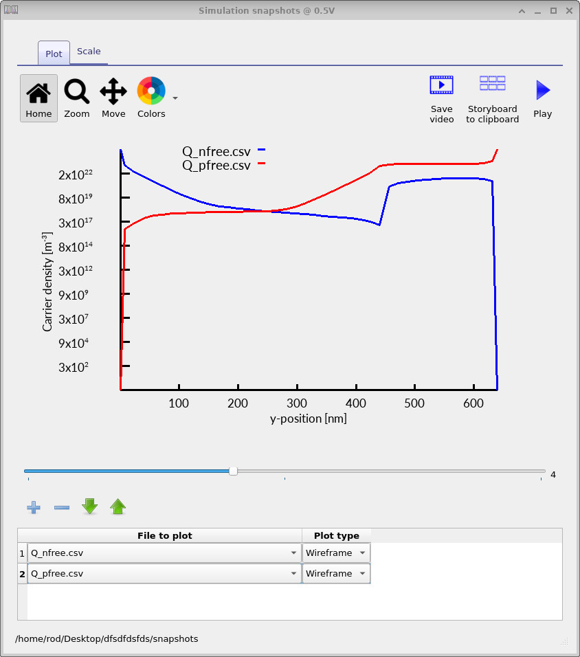
Inspect the JV curve as before. Then open the snapshots directory and plot the free electron and hole densities.
The result should resemble
??.
Instead of the 2D surfaces produced by the full electrical model, the carrier densities are now shown as
1D profiles through the layer stack.
This is often an efficient modelling strategy: retain 2D where the geometry requires it, but use 1D where the physics is predominantly through-thickness. The approximation is appropriate when lateral carrier transport is not important, as is often the case for laterally uniform thin-film solar cells.
9. Reducing the dimensionality of the optical problem
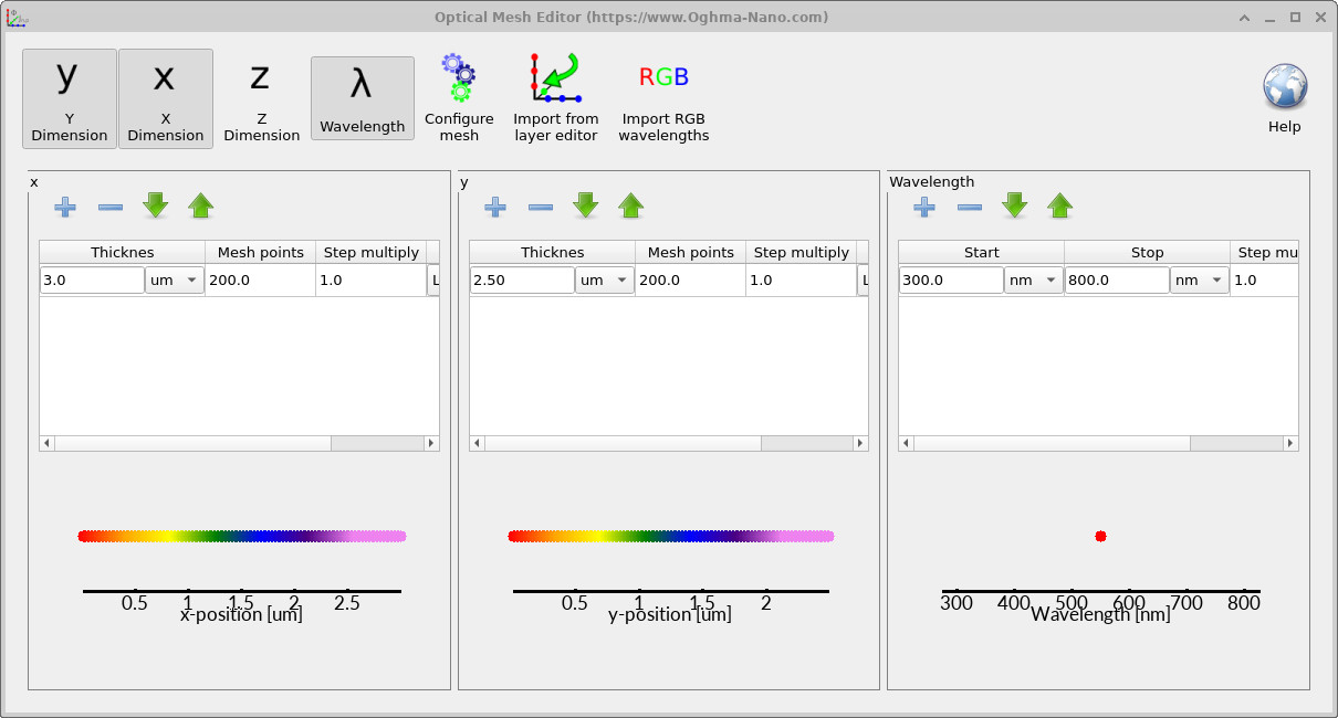
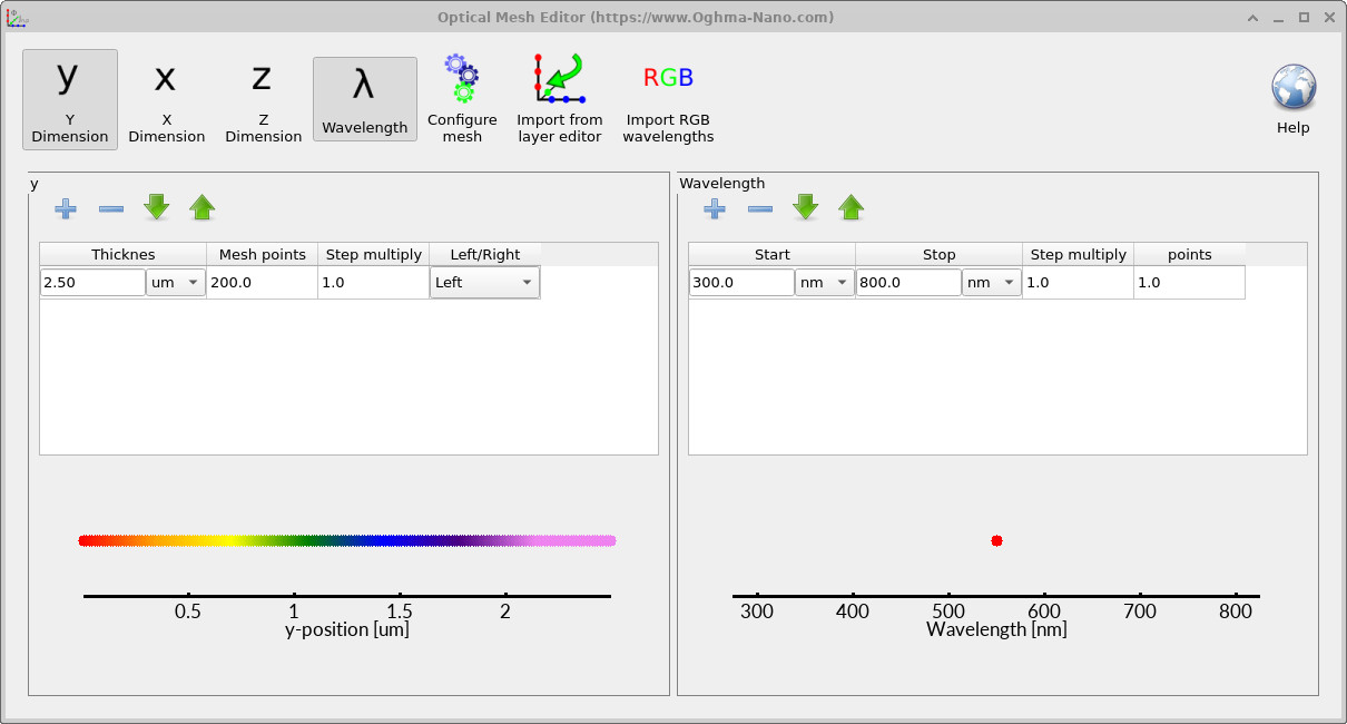
Having reduced the electrical problem, we can now do the same for the optical problem and see just how compact we can make the whole simulation. Go to the Optical ribbon, shown in ??, and click on Optical mesh. This opens the optical mesh editor, shown in ??. As with the electrical mesh, click the X Dimension button to remove the x discretisation. The optical problem is now solved in one dimension, as shown in ??, which shrinks the optical calculation dramatically.
While you are in the optical mesh editor, it is worth looking at the wavelength mesh on the right. You will see that the simulation is currently solving at only a single point in wavelength, placed roughly in the middle of the 300–800 nm range at around 550 nm (the same green wavelength we used for the FDTD run earlier). In other words, this example does not simulate the full solar spectrum - it evaluates the device at just one colour of light. If you wanted the complete solar-spectrum response, you would need to add many more wavelength points (at least around 20 to resolve the spectrum sensibly). That is perfectly possible and entirely valid, but the computational time would increase significantly, so we keep to a single wavelength here to keep the demo fast.
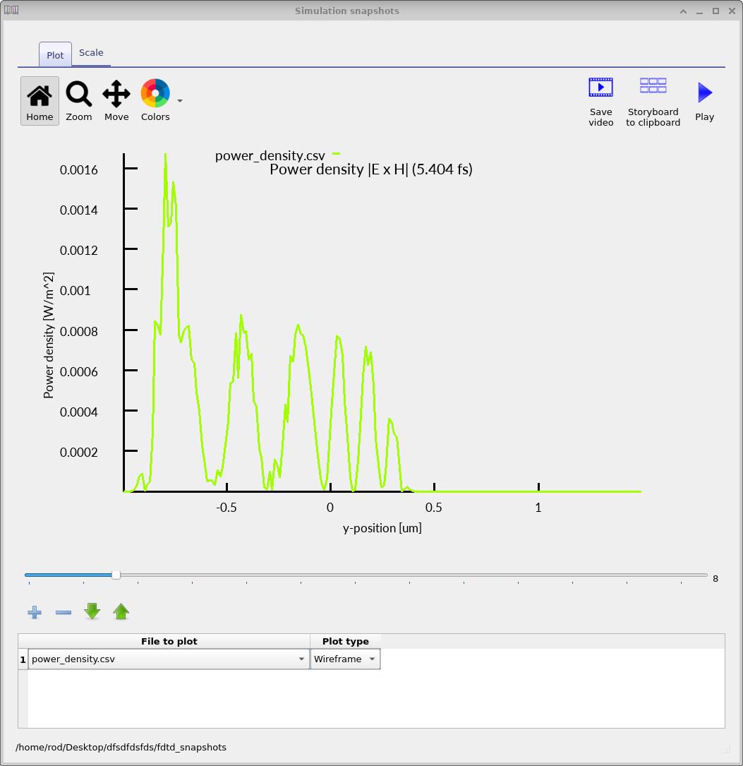
Now run the simulation again. At this point we have a 1D optical simulation coupled to a 1D electrical simulation - the most lightweight version of the model. You can inspect the 1D FDTD result from the snapshot viewer, as shown in ??. The optical power density is now a single 1D line profile as the pulse travels through the device, rather than the 2D field map we saw at the start of the tutorial.

10. A faster alternative: the transfer matrix method
To finish the tutorial, we will switch from FDTD - which, as we have seen, is very computationally intensive - to the much cheaper transfer matrix method (TMM). In most solar-cell tools the transfer matrix method is thought of as a strictly one-dimensional model, only really suited to flat, planar stacks. However, because of the way OghmaNano is organised, you can apply the transfer matrix model in any direction and in any dimensionality, which makes it a flexible drop-in replacement for FDTD in many situations.
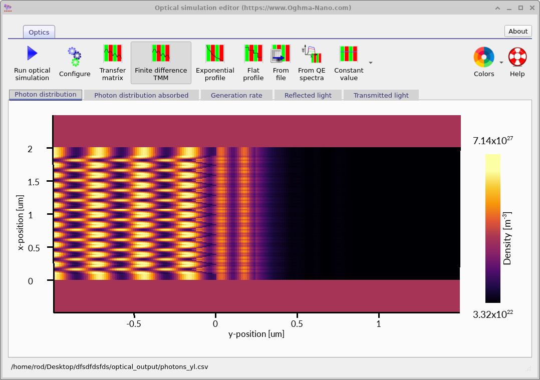
Go to the Optical ribbon and click on the Transfer matrix button. This opens the optical simulation editor shown in ??. Click Run optical simulation, and you will obtain a photon distribution much like the one shown there. What OghmaNano has done here is apply the transfer matrix method across the 2D device, solving it as a series of independent vertical slices down the structure. Crucially, unlike FDTD there is no cross-coupling between neighbouring slices: the transfer matrix method is a much simpler approximation of Maxwell’s equations, so light cannot scatter sideways from one slice into the next. In exchange for that approximation, it runs much, much faster than FDTD, because there is no time-stepping of the field.
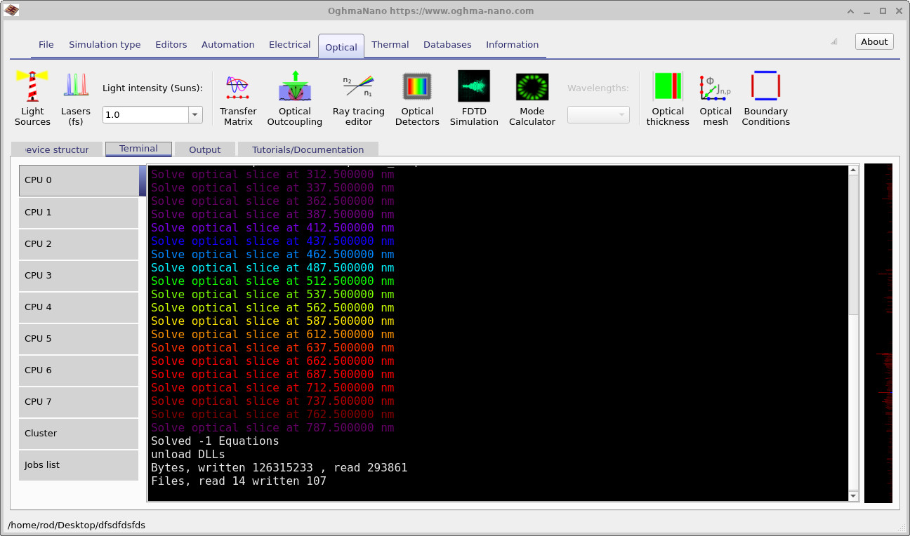
Because the transfer matrix method is so cheap, we can now afford to solve over many wavelengths rather than a single one. Go back to the Optical mesh editor and set the wavelength mesh to around 20 points, then rerun the optical simulation. While it is running you will see the terminal work through each wavelength in turn, as shown in ??. Each optical slice is solved at its own wavelength (here stepping from roughly 312.5 nm to 787.5 nm), and the text is colour-coded to indicate the wavelength currently being solved.
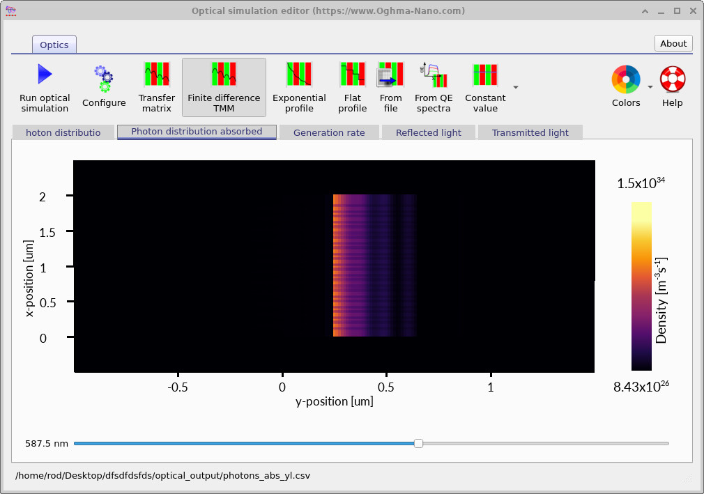
Once the run has finished, return to the transfer matrix window, ??, and select the Photon distribution absorbed tab. You can now use the slider along the bottom of the window to step through wavelength and see where in the device each colour of light is absorbed. In the example shown the slider is at 587.5 nm, and you can see the corresponding absorption profile inside the perovskite device. This is a quick and intuitive way to understand how different parts of the solar spectrum are absorbed at different depths in the cell.
11. Choosing the optical generation model
By default, this simulation uses the FDTD solver as its optical generation model - this is what feeds the
generation profile into the electrical calculation. If you would rather use the faster transfer matrix method to drive the
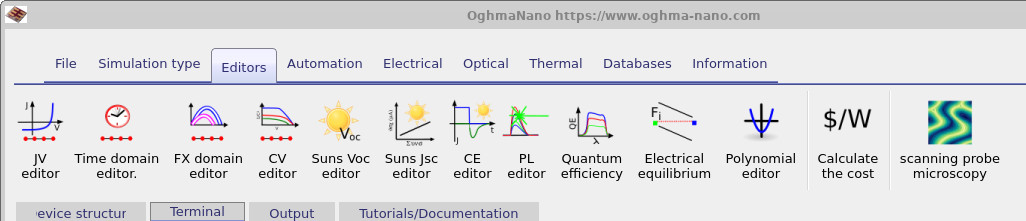
electrical simulation, you can change the generation model directly. Open the ribbon shown in
?? and click on the
JV editor. In the JV editor, under Charge carrier generation, change the Charge carrier
generation model from FDTD to transfer matrix, as shown in
??. From then on the optical
generation profile will be calculated with the transfer matrix method rather than with FDTD.
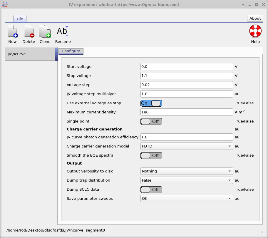
FDTD to transfer matrix.
Summary. Over the course of this tutorial we have taken a single device through a whole range of modelling choices. We started with a full 2D FDTD optical simulation coupled to a 2D drift-diffusion electrical model of a perovskite cell with a complex, light-trapping top surface. We then reduced the dimensionality of both the optical and the electrical problems from 2D down to 1D, watched the runtime and the results change, and brought them back up to 2D again. Finally, we simplified the optical problem in a completely different way, by replacing FDTD with the much faster transfer matrix method.