Bragg Grating Simulation (FDTD): 1D Bragg Mirror Tutorial
1. Introduction
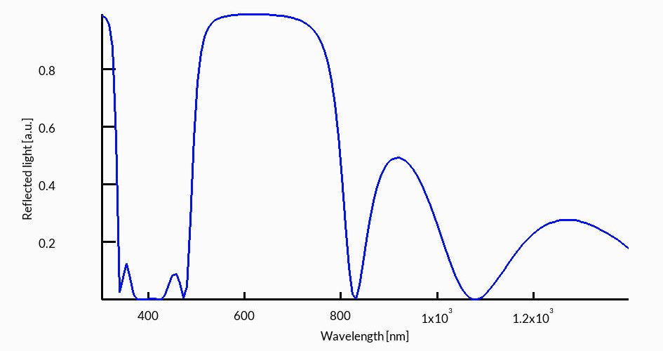
A Bragg grating (or Bragg mirror) is a simple periodic structure that reflects a narrow range of wavelengths. This behaviour is shown clearly in ??, where a strong stop band appears and transmission is suppressed.
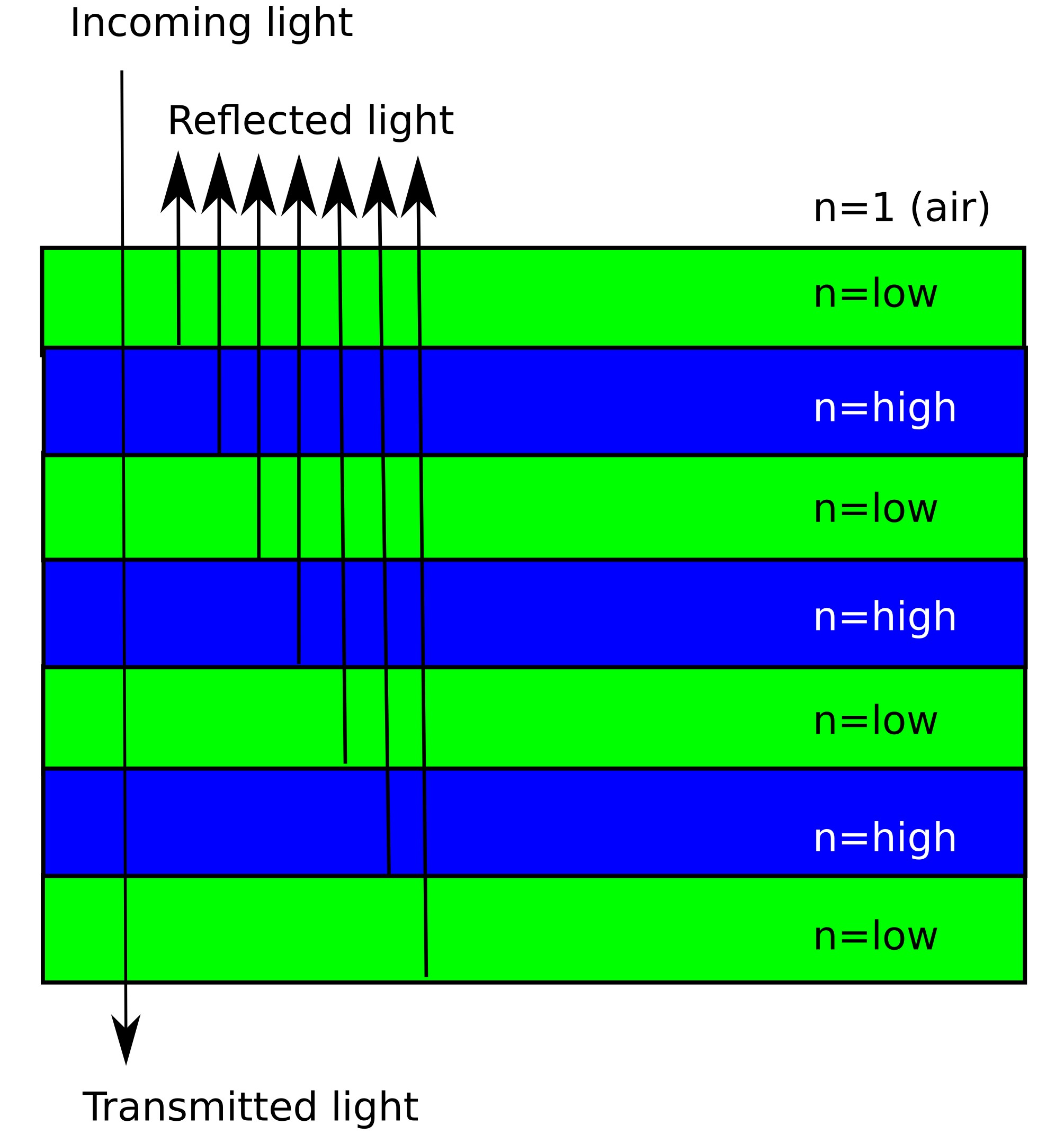
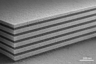
The structure consists of alternating layers of high-index and low-index materials, as illustrated in ?? and in the multilayer example shown in ??. When light encounters each interface, a small portion is reflected. These reflections can add together coherently, producing strong overall reflection.
To achieve this, the layer thicknesses are chosen carefully. In a standard quarter-wave design, each layer has an optical thickness of one quarter of a target wavelength \(\lambda_0\), so that \(n_1 d_1 = \lambda_0/4\) and \(n_2 d_2 = \lambda_0/4\). This ensures that reflections from successive layers return in phase and reinforce each other.
In this tutorial, we use the Finite-Difference Time-Domain (FDTD) method to simulate a simple 1D system with the layout PML | air | Bragg stack | air | PML. A broadband pulse is launched at normal incidence, and we measure the reflected and transmitted spectra. Later, we will extend this to higher dimensions, where the field behaviour becomes much richer, as illustrated in ??.
The key idea is that a Bragg grating is not just “many reflections”, but a periodic optical structure in which certain wavelengths cannot propagate efficiently. This is the simplest example of a 1D photonic crystal.
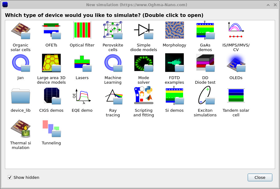
2. Making a new simulation
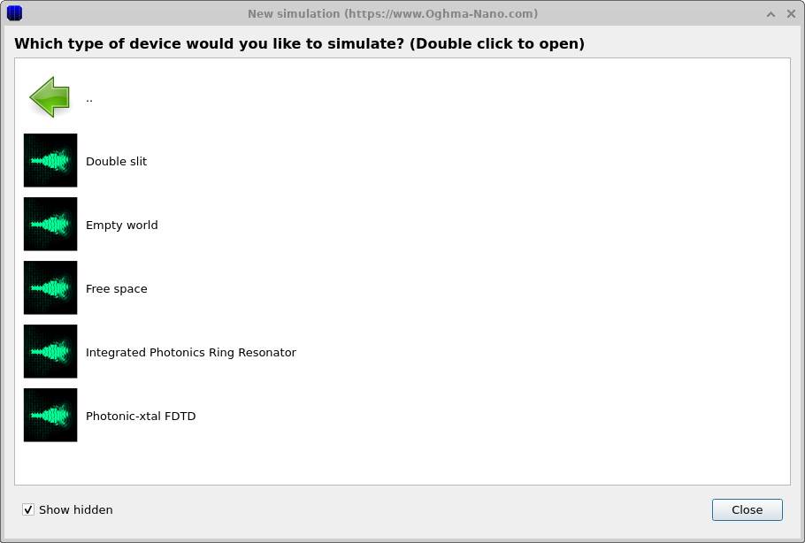
Open the New simulation window and select the FDTD examples category (??). Then choose the Bragg grating (1D) example (??). This loads the main interface shown in ??.
3. Orienting yourself in the main window
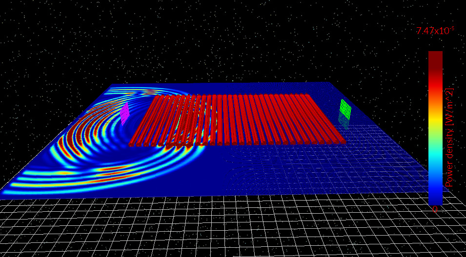
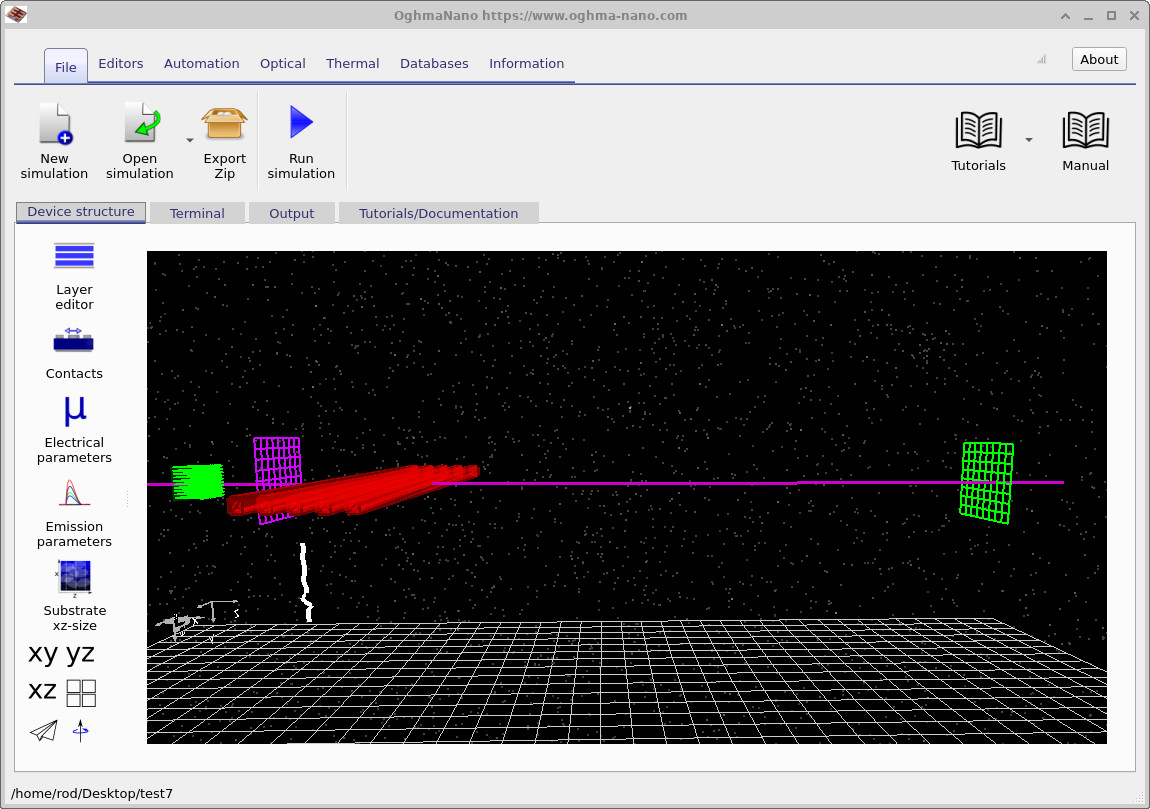
After loading the simulation, the main window will appear as shown in ??. The structure is displayed in the 3D view in the Device structure tab. In this view, you can see the key elements of the simulation. On the left, the block of green arrows represents the FDTD source, where the excitation is applied. A purple line runs through the structure, representing the FDTD grid. In this case it is a 1D simulation, so the grid is a single line passing through the grating.
You can also see a purple grid, which represents the input detector plane. Light from the source passes through this detector before reaching the grating. The grating itself is shown in red, forming the periodic structure at the centre of the simulation. On the right-hand side, there is a second detector plane shown in green. This is the output detector, which captures the light that has passed through the structure.
It should be noted that the detectors do not interfere with the light itself; they simply measure the electromagnetic fields.
In a moment, we will run the simulation and observe how light travels through the structure and interacts with the Bragg grating. You will see how the wave is partially reflected and transmitted, and how this behaviour is recorded by the two detectors on either side of the structure.
4. Running the simulation
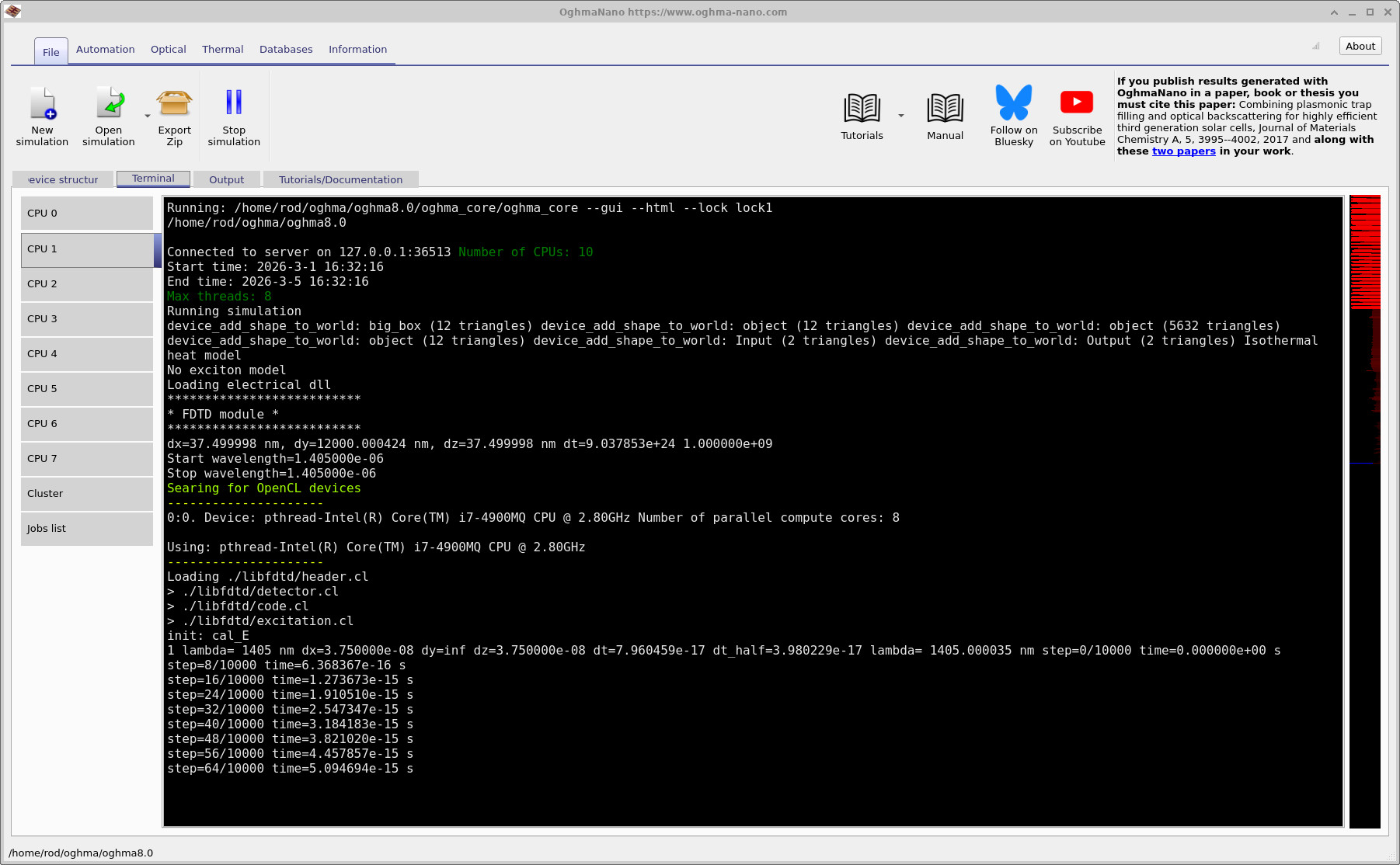
Once you have saved the simulation and had a look around the structure, click the Run (▶) button to start the calculation. As the simulation runs, you can monitor its progress in the Terminal tab, shown in ??. This displays information such as the timestep, wavelength range, and backend being used. When the simulation has finished, switch to the Output tab, shown in ??. Here you will find the data generated during the run.
The key outputs for this tutorial are detector_0 and detector_1, which contain the signals recorded by the two detectors.
You can also open device to view the 3D geometry, and the snapshots/ directory to see how the electromagnetic fields evolve over time. You should notice that this simulation runs very quickly. Because it is a 1D problem, typical run times are only a few seconds. If the simulation is taking significantly longer than this, refer to the note above about saving the simulation on a fast local drive.
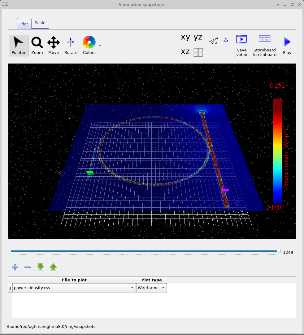
5. Viewing power density snapshots
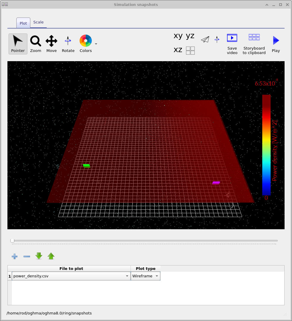
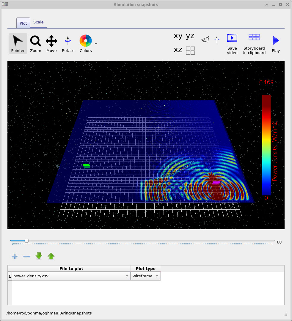
Open the snapshots/ output directory (from the Output tab) and double-click to launch the snapshot viewer.
This allows you to view the simulation results as a function of time.
Click the + button once to add a dataset, then select Ey. In this simulation the field is excited in the
y-direction, so this component gives the most informative view of the wave propagation.
You can then use the slider bar to step through time and observe how the field evolves. Three representative snapshots are shown in
??–
??.
You will see a broadband pulse propagate through the input region, interact with the Bragg grating, and reflect strongly, with only a small portion of the field penetrating into the multilayer. This provides a direct, time-domain view of how the stop band emerges from the wave dynamics.
You can also plot the power density if you prefer, which is proportional to the product of the electric and magnetic fields. More precisely, this corresponds to the Poynting vector, \(\mathbf{S} = \mathbf{E} \times \mathbf{H}\), which represents the flow of electromagnetic energy.

6. Viewing detector outputs
Returning to the Output tab (see
??),
you will see two detector folders, Detector0 and Detector1, which appear like small camera icons.
Detector0 is located on the source side of the Bragg grating, while Detector1 is on the far side after the light has passed through the structure. If you double-click on Detector0, you will see the contents shown in
??.
In this directory there are two files, lam_e.csv and power.csv.
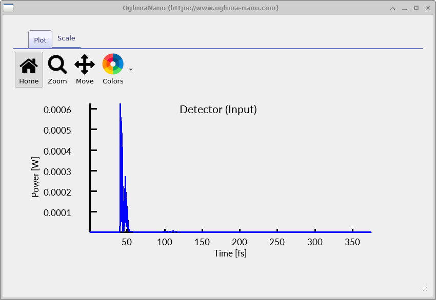
For now, open power.csv, which shows the power passing through the detector as a function of time.
The result is shown in
??.
This is a plot of the power recorded at the input-side detector. You can see that at around 50 fs,
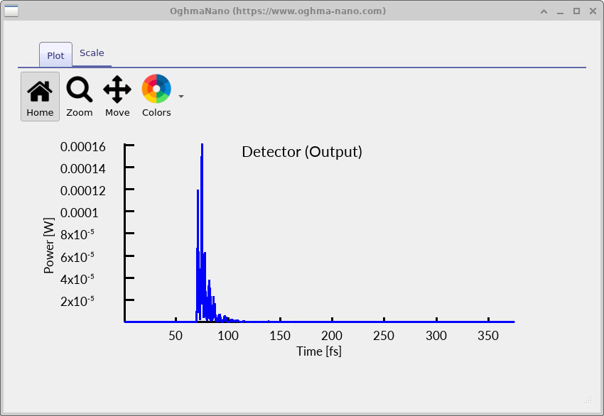
a packet of light reaches the detector. You can now repeat the same process for Detector1. Opening power.csv in that folder gives the result shown in
??.
In this case, the same packet of light arrives at the second detector roughly 25 fs later, after passing through the Bragg grating.
You should also notice that the shape of the power signal has changed after transmission through the structure. This reflects how the Bragg grating modifies the wave as it propagates through the multilayer.
lam_e.csv and power.csv.
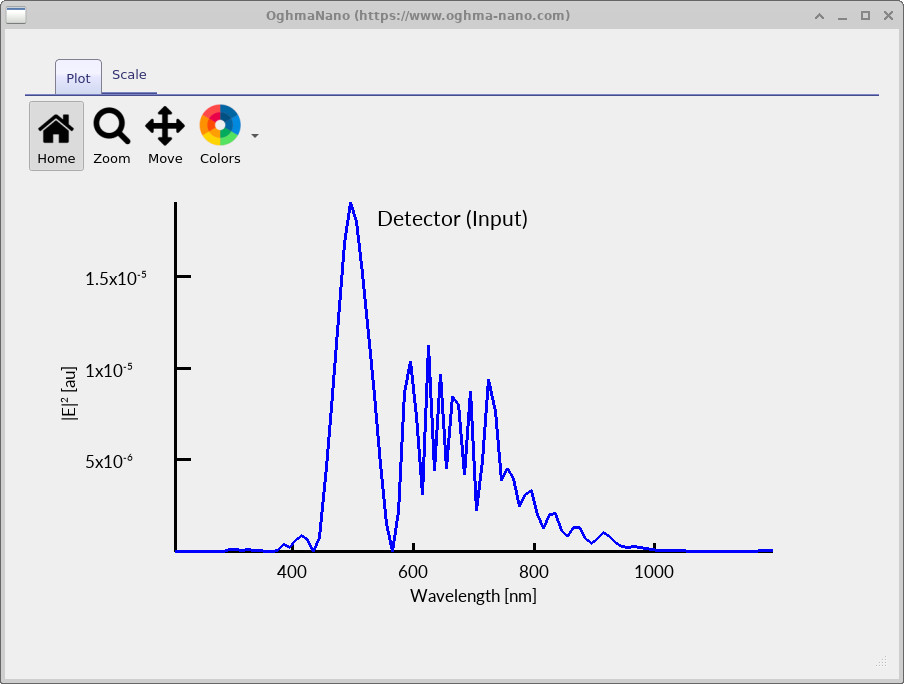
We can now move from the time-domain signals to the frequency-domain response. The signals shown previously can be
Fourier transformed to give the spectral content of the light passing through each detector. The frequency-domain data can be found in the file lam_E.csv inside both Detector0 and Detector1.
Input spectrum: The input-side spectrum is shown in ??. In this simulation, the source is a Gaussian pulse with a carrier wavelength of 500 nm, so the spectrum is centred around this value. This shows the frequency-domain representation of the signal recorded at Detector0. You can see a strong peak near 500 nm, corresponding to the main excitation. The surrounding structure in the spectrum, which may appear somewhat irregular or “messy”, arises from several effects. First, the pulse has a finite duration, which means it contains a range of wavelengths rather than a single frequency. Second, the reflected wave from the Bragg grating interferes with the incoming wave at the input-side detector, producing additional structure in the spectrum. Finally, small oscillations can also arise from the finite simulation length and the discrete nature of the Fourier transform. In this case, the linear scale is the most useful, as it clearly shows the dominant excitation peak.
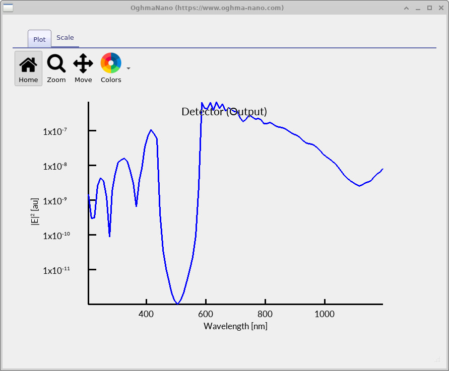
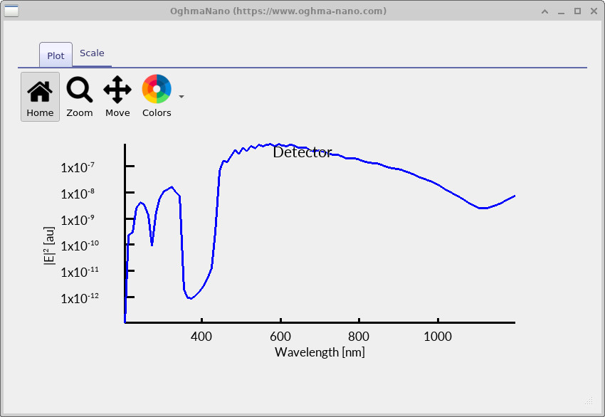
Output spectrum: The corresponding output-side spectrum is shown in
??.
This shows the spectral content of the light after it has passed through the Bragg grating. Compared to the input spectrum, the most obvious feature is the strong dip around 500 nm.
This is the key effect of the Bragg grating: it suppresses transmission at the design wavelength.
Outside this region, the signal is transmitted more efficiently. It is often useful to switch the vertical axis to a logarithmic scale (by pressing the l key while the graph is selected),
as this makes it easier to see weaker features in the transmitted signal. On a linear scale, the dominant behaviour is clear,
but the log scale reveals additional structure across the spectrum.
Input/output ratio: The key result is that although the system is excited near 500 nm, the output shows a
strong suppression at this wavelength. This means the Bragg grating is effectively blocking the 500 nm component of the
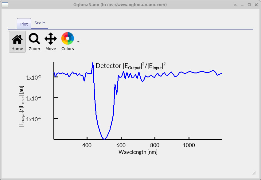
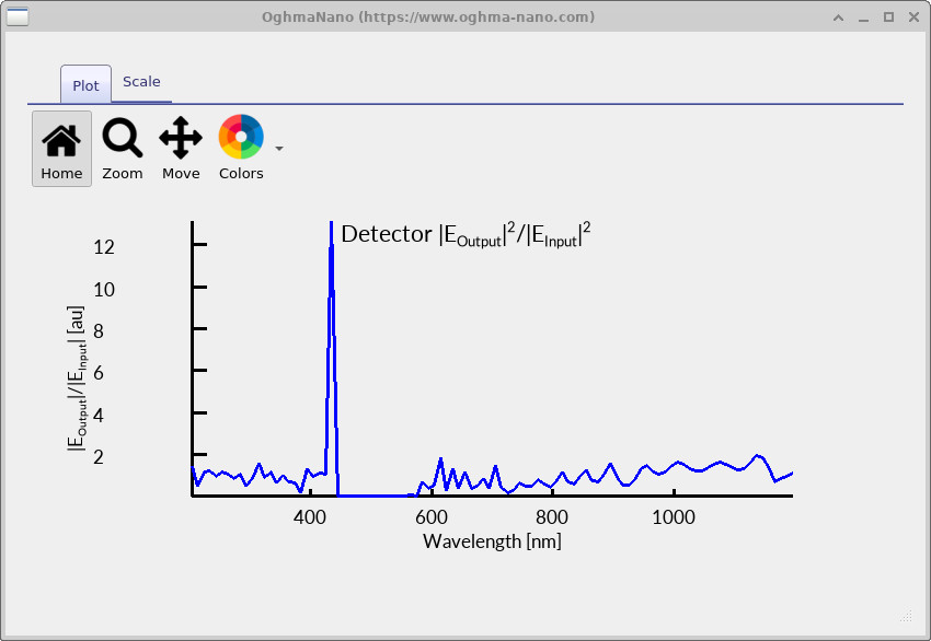
incoming light. To quantify this, we take the ratio of the output and input signals. Since power is proportional to \(|E|^2\), this gives the
transmission of the structure:
\(T(\lambda) = \frac{|E_{\mathrm{output}}(\lambda)|^2}{|E_{\mathrm{input}}(\lambda)|^2}\).
The result is shown in
?? and
??,
where the suppression around 500 nm is clearly visible. A logarithmic scale is often more useful here, as it shows the depth of the stop band and weaker transmission features more clearly (press l with the graph selected to toggle between linear and log scale).
The spikes/oscillations in the \(T(\lambda)\) spectrum can be quite pronounced in places. These arise from the finite duration of the pulse, interference within the stack, and the fact that the frequency-domain signal is constructed from a finite time window. They are a normal feature of this type of simulation. For a cleaner transmission spectrum, a separate reference simulation without the grating can be used for normalisation, but this is not required to see the main effect here.
7. Experimenting with the grating dimensions
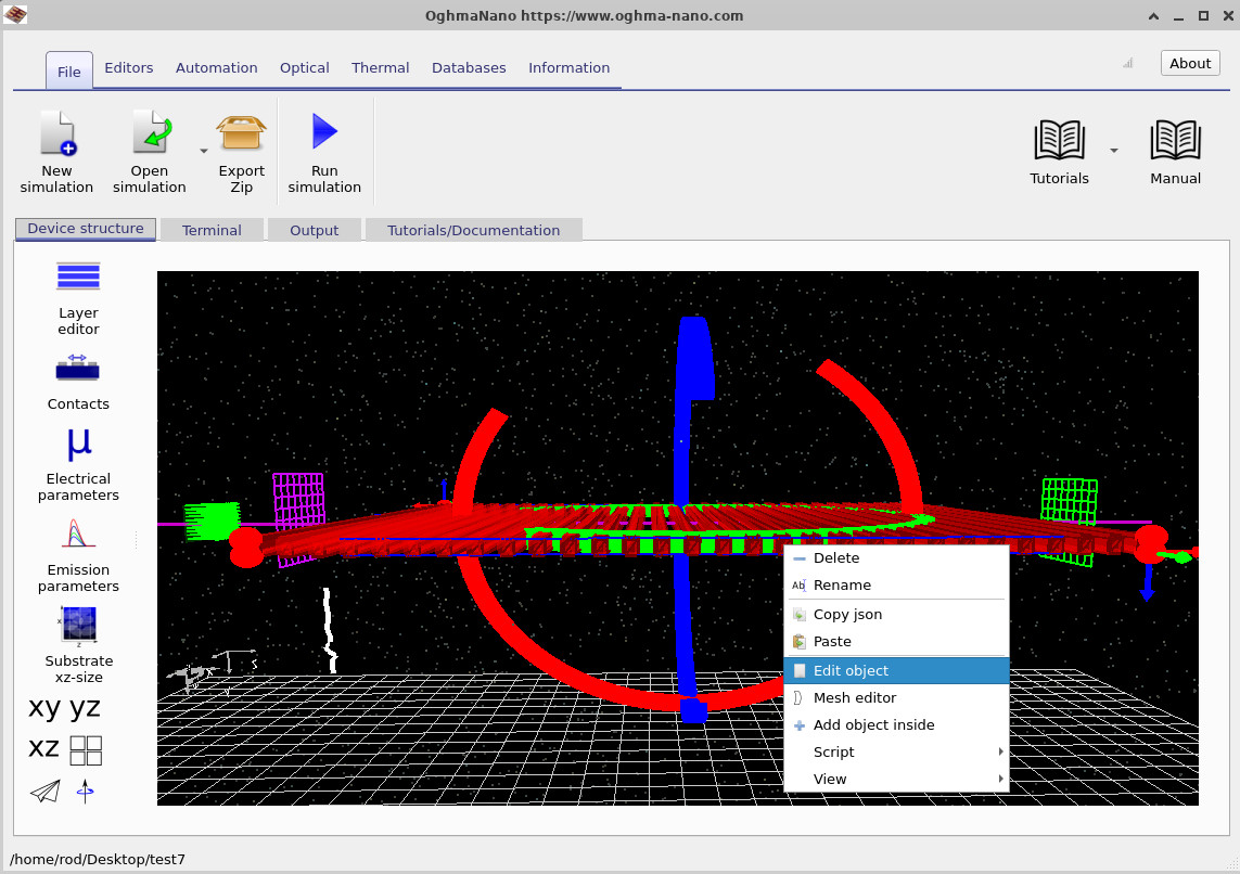
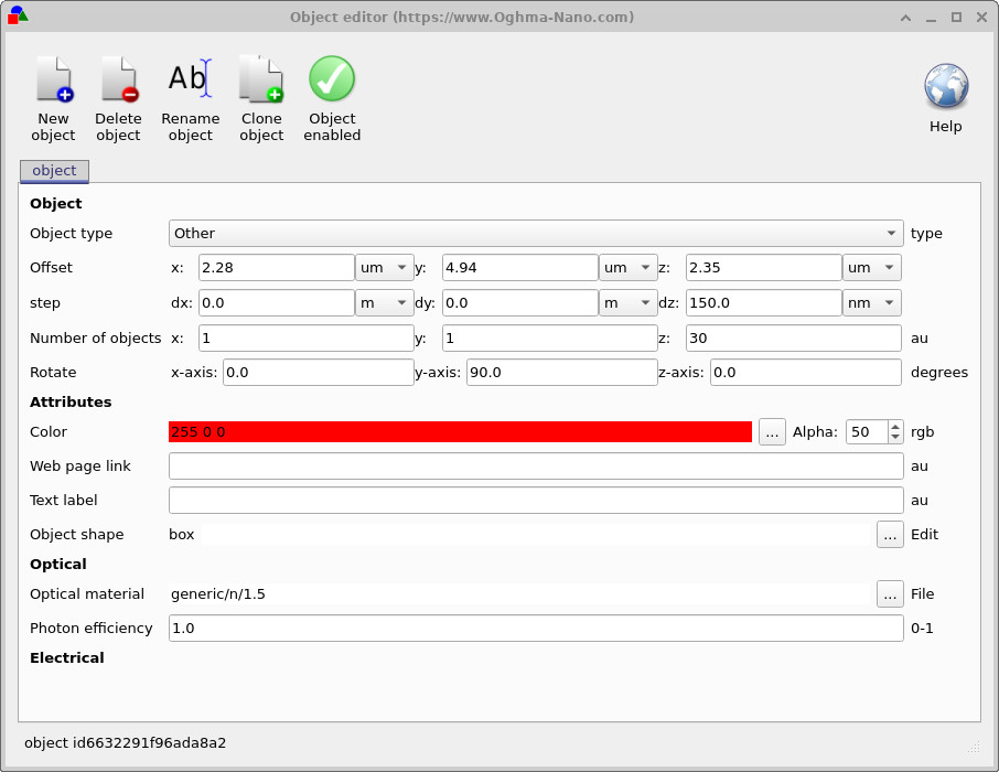
To explore how the Bragg grating behaviour depends on its structure, right-click on the grating and select Edit object, as shown in ??. This opens the object editor, where the size and repetition of the grating can be controlled.
The Offset fields define the position of the object in \(x\), \(y\), and \(z\), while the Number of objects setting controls how many repeated elements are created. In this model, a single bar is defined and then copied multiple times to form the grating. This allows one set of material properties to be reused across many periods. Initially, the number of objects in the z direction is set to 30. Change this to 5, as shown in ??. After applying this change, the structure should look like ??, where the number of grating periods has been significantly reduced.
Now rerun the simulation and inspect the output spectrum. The result is shown in ??. You should see that the notch around 500 nm is much less pronounced. This is because a shorter grating provides weaker constructive interference and therefore weaker reflection at the design wavelength.
If you now increase the number of periods again (for example to 20 or 30), rerun the simulation, and examine the output spectrum, you will obtain a result similar to ??. In this case, the stop-band around 500 nm becomes much stronger again.

Number of objects to 5.

8. Changing the period of the grating
You can also control the spacing between the grating elements. Right-click on the grating and select
Edit object as before. Ensure that the number of objects in the \(z\)-direction is set to 30,
but now change the dz step to 150 nm, as shown in
??.
After applying this change, the grating elements will move closer together, effectively reducing the period of the structure. Rerun the simulation and inspect the output detector spectrum. The result is shown in ??.
You should see that the position of the stop band has shifted compared to the previous case. This is because the Bragg condition depends on the grating period: reducing the spacing changes the wavelength at which constructive interference occurs, and therefore shifts the wavelength that is strongly reflected.
dz step (here 150 nm).
9. Extending to 2D
One of the strengths of the FDTD method is that it is straightforward to extend simulations to higher dimensions. So far, we have considered a 1D problem, where the fields vary only along the propagation direction. We will now extend this to 2D and observe how the fields behave when variation in a second spatial dimension is allowed.
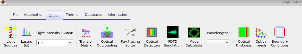
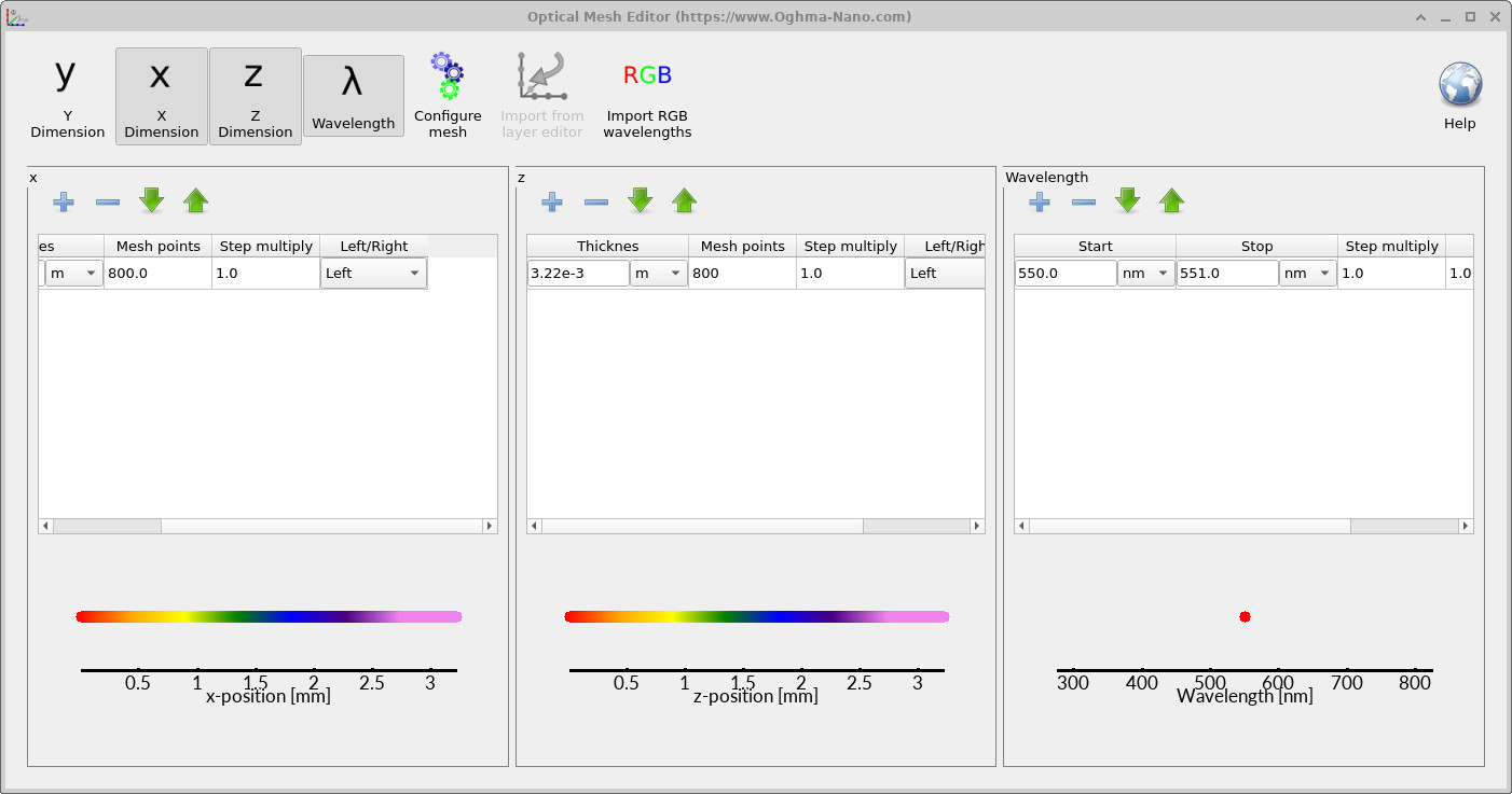
To do this, go to the Optical ribbon, shown in ??, and click on the optical mesh editor.
This will open the mesh editor, where the spatial discretisation of the simulation is defined. The current setup only includes variation along the z direction. To extend the simulation to 2D, click on the x dimension tab, as shown in ??. This activates variation in the x-direction and expands the simulation domain from 1D to 2D.
After enabling the x dimension, rerun the simulation. You will notice that the runtime increases significantly (typically from a few seconds to several minutes). This is expected: increasing the dimensionality increases the number of grid points and therefore the computational cost. This is the trade-off in FDTD—greater physical realism comes at the cost of longer simulation times.
Once the simulation has completed, open the snapshots/ directory and view the results. Example field
distributions are shown in
??–
??.
Using the slider bar, you can step through time and observe how the fields propagate and scatter in two dimensions.
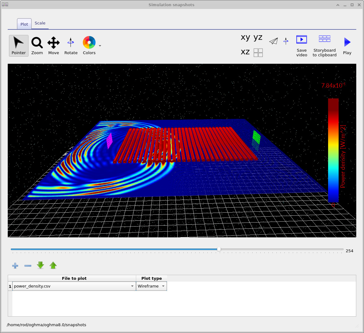
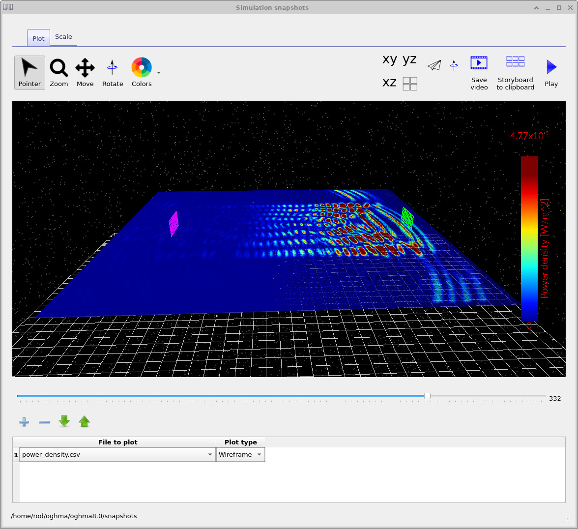
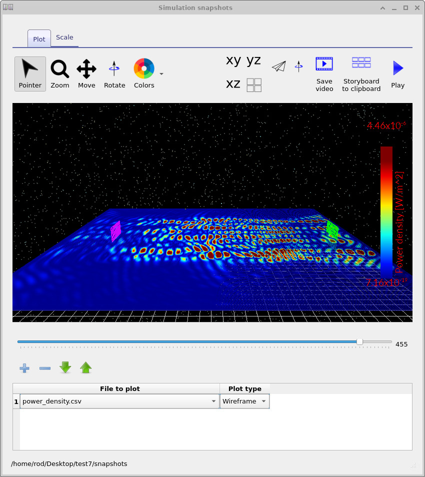
Compared to the 1D case, the fields now exhibit lateral spreading and more complex interference patterns. This highlights an important point: while 1D simulations capture the basic physics of Bragg reflection, higher-dimensional simulations reveal additional effects such as diffraction and spatial mode structure. These become essential when modelling real devices.