Tapered GaAs Waveguide (FDTD): Mode Expansion and Stability Tutorial
1. Introduction
Tapered waveguides are used to expand light in a controlled way. In a narrow waveguide, the optical mode is tightly confined and the power density can become very high. By gradually widening the structure, the mode can spread over a larger area, reducing the optical intensity while still carrying substantial total power. This is important in high-power photonic devices such as laser diodes, where excessive facet intensity can contribute to catastrophic optical damage and other unwanted high-field effects.
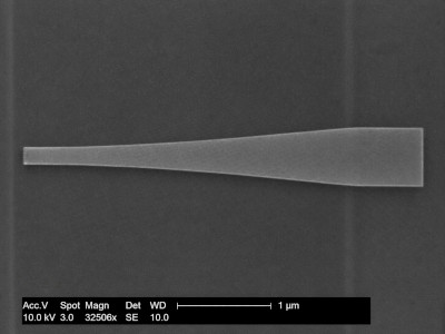
The tapered structure studied in this tutorial is shown in ??, while the corresponding optical field expansion is shown in ??. The device is a GaAs waveguide designed for 975 nm. Light is launched into the narrow section and then propagates into the wider flare, where the mode expands as the available guiding region increases.
This makes tapered waveguides useful for two reasons. First, they can improve coupling between a tightly confined waveguide mode and a larger optical component. Second, they can lower the power density at a device facet by increasing the mode area before the light reaches the output. In practical terms, this means the taper can help a device handle more optical power without concentrating that power into such a small region.
In this tutorial, you will run a tapered-waveguide FDTD simulation, inspect the field snapshots, and then widen the flare to see how the behaviour changes. You will find that making the taper wider does not always improve the result. If the geometry becomes too broad, the field can no longer remain in one clean expanding mode and instead begins to excite a more complicated set of waveguide modes. This gives a direct and visual introduction to mode expansion, taper design, and modal stability in FDTD waveguide simulations.
2. Making a new simulation
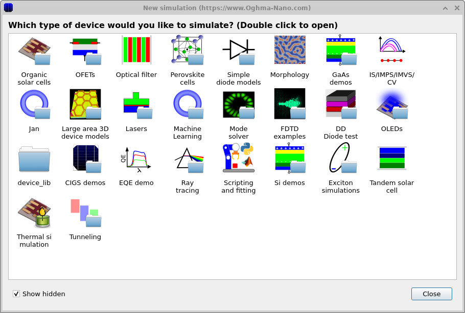
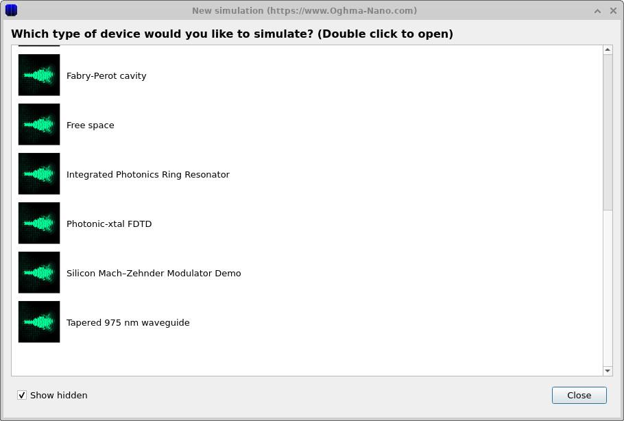
Open the New simulation window and select the FDTD examples category (??). Then choose the Tapered 975 nm Waveguide example (??). This loads the main interface shown in ?? and ??.
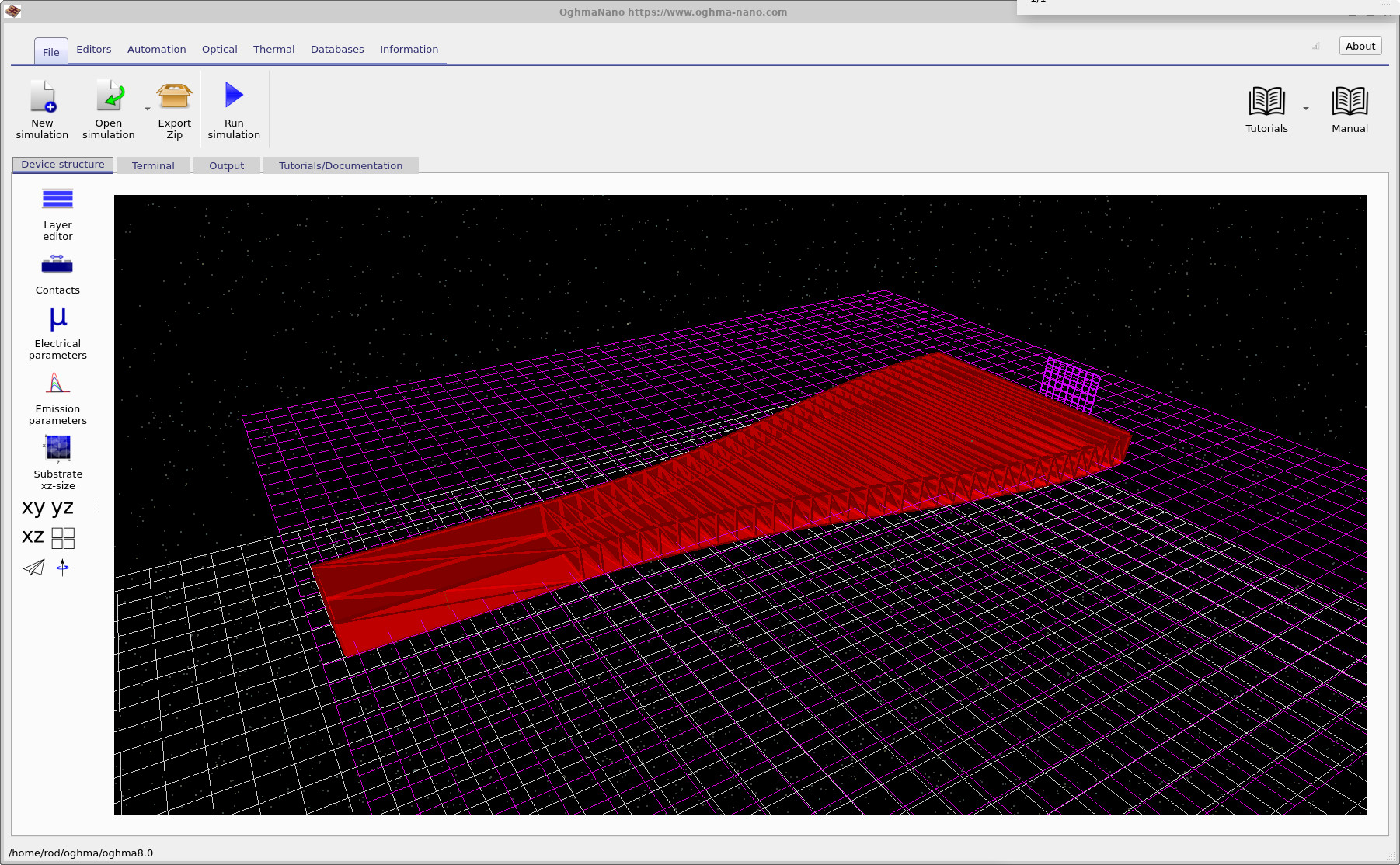
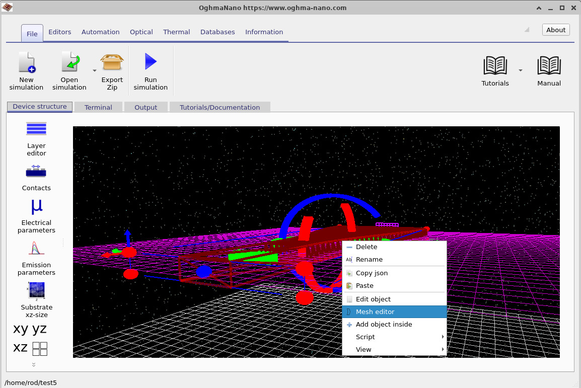
Save the simulation to a new directory of your choice. Once loaded, the structure is displayed in the Device structure tab. The default three-dimensional view is shown in ??. The red tapered object is the GaAs waveguide. The green rectangle inside the narrower section is the FDTD optical source, and the purple plane near the output side is the detector.
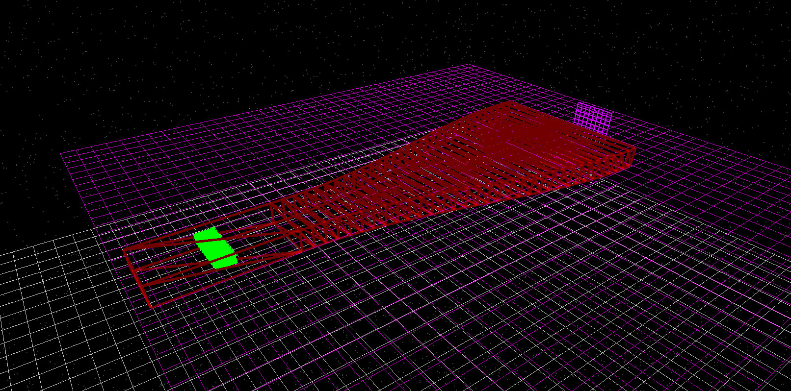
To see inside the structure more clearly, right-click on the tapered waveguide, open the View submenu, and untick Show solid. This produces the see-through view shown in ??. This view is useful because it lets you confirm that the optical source sits inside the waveguide volume and that the detector lies on the purple two-dimensional FDTD plane. That plane is the active simulation plane, so both the optical source and the important parts of the geometry must lie within it for the calculation to make physical sense.
3. Running the simulation
Click the Run (▶) button to start the FDTD simulation. As in the other FDTD examples, OghmaNano will automatically search for any suitable OpenCL devices and use hardware acceleration if it is available. Because this example is compact and the geometry is already prepared, it runs quickly and is well suited to parameter exploration.
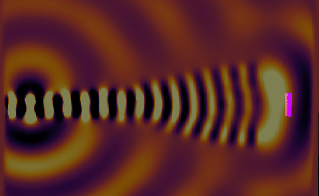
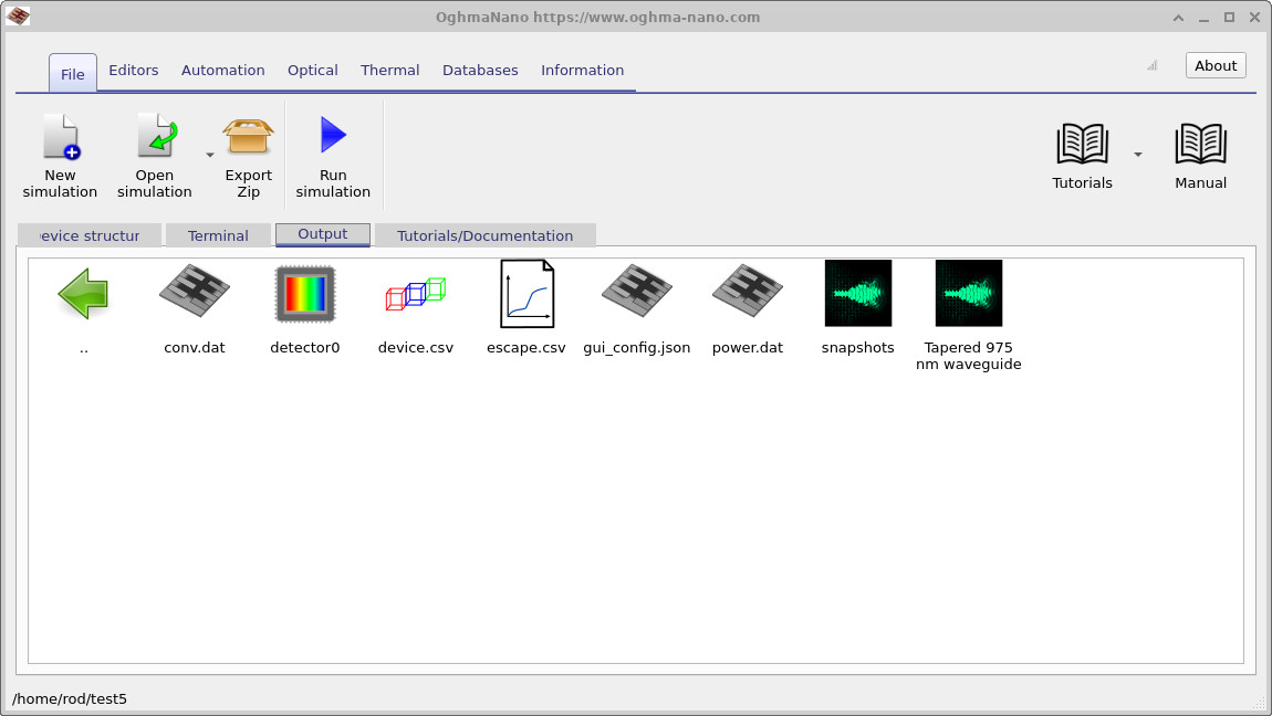
When the run has finished, switch to the Output tab shown in ??. The most important outputs for this tutorial are the snapshot files, which allow you to inspect how the optical mode evolves as it travels along the taper. The simulation has been arranged so that the field is launched within the narrow section of the guide and then propagates into the flared section.
4. Viewing electric field snapshots
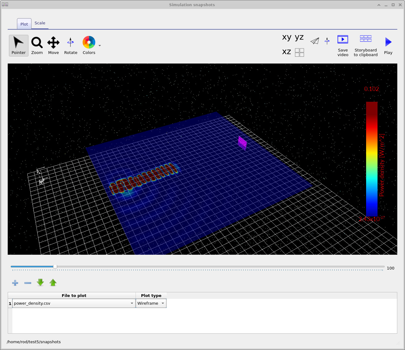
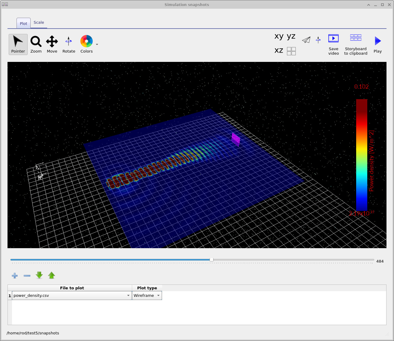
Open the snapshots/ output directory from the Output tab and launch the snapshot viewer. Three representative frames are shown in
??,
??, and
??.
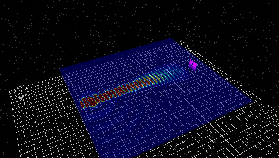
In the first snapshot (??), the optical field is still mainly confined in the narrower section of the waveguide. The power density is concentrated and the mode occupies only a relatively small part of the structure.
In the second snapshot (??), the field has propagated further into the flared region. The mode begins to occupy a larger area, and the energy is distributed over a wider cross-section of the waveguide. This is the central effect that makes tapered structures useful in high-power devices: the optical mode can spread out spatially instead of remaining tightly concentrated.
By the third snapshot (??), the field has expanded significantly within the taper. The mode is visibly broader than in the input section. In a real device, this broader optical distribution reduces the local intensity at critical interfaces such as output facets. In a laser diode, lowering the facet intensity can help suppress catastrophic optical damage and can reduce the strength of parasitic thermal and refractive effects associated with strongly concentrated fields.
5. Editing the taper geometry
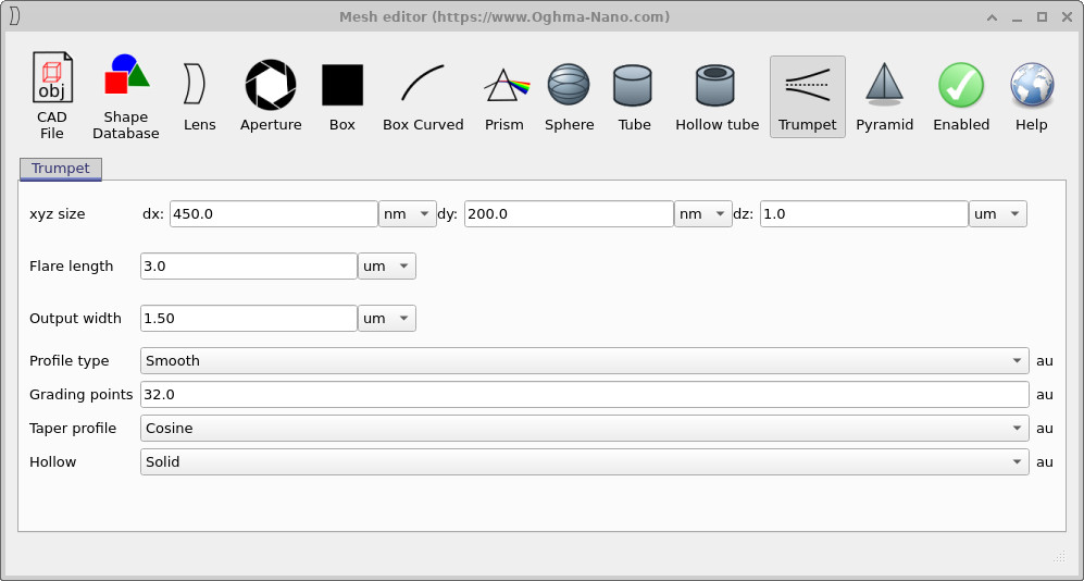
We now modify the taper itself so that the output flare becomes wider. Return to the Device structure tab, right-click on the tapered waveguide, and choose Mesh editor, as shown in ??. This opens the taper mesh editor shown in ??.
In the editor, change the Output width from 1.50 µm to 3.0 µm. Leave the rest of the settings unchanged and apply the modification. This increases the width of the flare and therefore changes the optical modes that the wider section of the waveguide can support.
After changing the taper geometry, the optical source will no longer sit correctly inside the waveguide. Because the shape of the tapered object has changed, the source must be moved manually so that it once again lies within the cavity. Drag the source into the guide, using the Shift key if necessary to move it through objects. Rotate the three-dimensional view to confirm that the source is actually embedded in the waveguide and not offset above or below it. It is also important that the source remains on the purple two-dimensional FDTD plane, otherwise it will not couple correctly into the simulation.
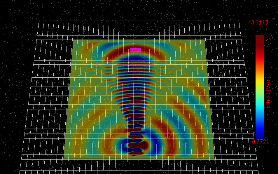
Once the source has been repositioned, rerun the simulation. The resulting field pattern is shown in ??. At first glance it may seem surprising that making the taper wider does not simply produce a cleaner, broader mode. Instead, the field begins to look less stable. The reason is that the wider section of the waveguide supports a larger family of lateral field distributions, while the square source launched inside the narrow region is not a perfect match to one single eigenmode of the widened structure. As the field enters the broader region, it can therefore redistribute into a mixture of allowed modes. These modes interfere with each other and can produce lateral asymmetry, oscillation, and a less controlled spatial expansion.
In other words, the optical field is not simply “filling” the wider waveguide in a uniform way. The field must still satisfy the modal structure imposed by the refractive-index profile and the boundaries. If the taper is widened too much, or widened too quickly, the field cannot remain in one clean fundamental-like mode and instead evolves into a more complicated superposition. This is why the output appears less stable in the wider case even though the physical structure is larger.
6. Interpreting the physics
The default simulation shows the regime in which the taper is able to broaden the mode in a controlled way. The field starts in a relatively confined section, then expands as the available mode area increases. In physical terms, the taper provides a gradual change in boundary conditions, allowing the propagating field to adapt as it moves forward.
The modified simulation with the larger flare width shows the limitation of that picture. Once the wider section can support more complicated transverse field shapes, the optical excitation no longer maps cleanly onto one dominant mode. The launched field is square rather than perfectly mode matched, so the wider taper does not simply receive a smooth broadened replica of the input mode. Instead, it receives a field with a finite distribution of transverse spatial frequencies. In the wider section, that distribution can project onto several supported modes. The beating and interference between those modes produces the unstable-looking pattern seen after the geometry is changed.
This behaviour is important in real photonic design. It means that increasing the physical width of a taper is not automatically beneficial. A broader output can indeed reduce local power density, but only if the mode remains controlled while it expands. If the geometry becomes too wide or too abrupt for the launched field, then part of the benefit is lost because the optical power is redistributed into unwanted modal structure rather than into one clean expanded mode.
7. Conclusion
In this tutorial you have created a tapered GaAs waveguide operating at 975 nm, run an FDTD simulation, and inspected the field snapshots showing optical mode expansion inside the taper. You then edited the taper width and observed that a larger flare can destabilise the output mode rather than simply improving it. The reason is that the wider section supports a richer modal spectrum, while the square source used here excites the structure in a non-ideal way.
This makes tapered waveguides an excellent example of practical photonics design. They are useful because they can reduce power density and help manage high optical powers, but their performance depends critically on both geometry and excitation. A good taper is therefore not just one that is wider, but one that allows the field to evolve into the desired spatial distribution without exciting unwanted modes.