Tilted Facet GaAs Waveguide (FDTD): Optical Outcoupling Tutorial
1. Introduction
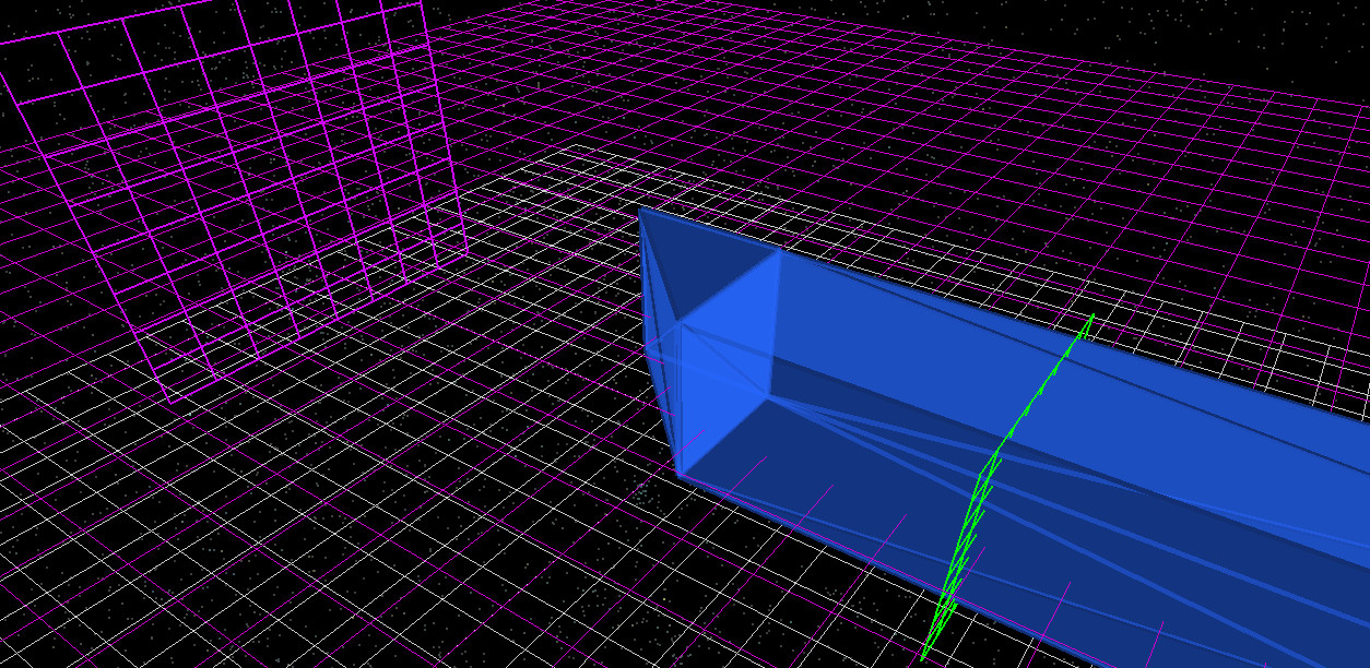
In photonic devices, optical power is generated or transported within high-refractive-index materials such as gallium arsenide (GaAs), where it propagates as a guided mode. To be useful, this guided power must be transferred across a dielectric boundary and coupled into free-space radiation. The simplified structure used to study this process is shown in ??, consisting of a subwavelength GaAs waveguide, an internal optical source, and a detector placed beyond the output facet.
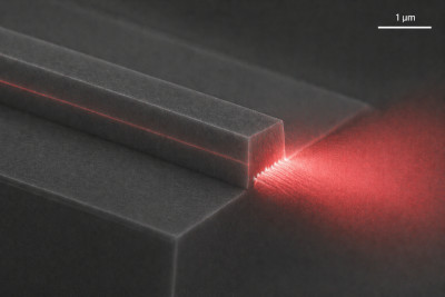
A concrete example is a semiconductor laser, in which light propagates along a waveguide and exits through the end facet, as illustrated in ??. At this interface, the guided mode encounters a refractive index discontinuity between the high-index waveguide and the surrounding medium. The reflected fraction is given by \( R = \left(\frac{n_1 - n_2}{n_1 + n_2}\right)^2 \), where \(n_1\) and \(n_2\) are the refractive indices of the waveguide and the external medium, respectively. For materials such as GaAs, this index contrast is large, so a significant fraction of the optical power is reflected back into the waveguide rather than being emitted.
One established method to modify this behaviour is to tilt the output facet. Introducing an angled interface alters the boundary conditions experienced by the guided mode, changing how power is partitioned between reflection, transmission, and scattering into radiation modes.
In this tutorial, we use the Finite-Difference Time-Domain (FDTD) method to model this process in a controlled geometry. A GaAs waveguide terminated by an angled facet is simulated, and the resulting optical field is analysed as it propagates and exits the structure.
We compare three cases:
- a shallow angled facet,
- a steeper angled facet, and
- a flat facet.
By comparing the detector output from these simulations, you will quantify how facet geometry controls the conversion of guided optical power into free-space radiation.
2. Making a new simulation
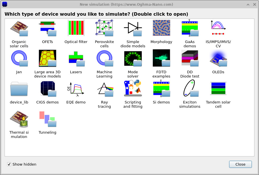
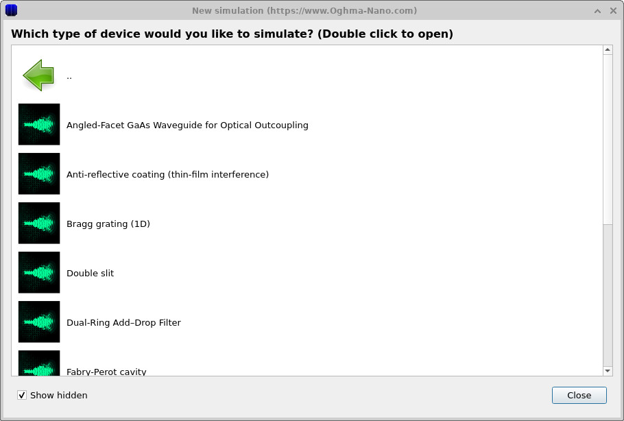
Open the New simulation window and select the FDTD examples category (??). Then choose the Angled Facet GaAs Waveguide for Optical Outcoupling example (??). This loads the main interface shown in ?? and ??.
Save the default simulation to a new directory called 40. It is important to use this exact name, because later in the tutorial you will create additional simulations with different facet geometries and directly compare the results between them.
In this naming scheme, the directory name corresponds to the dx dimension of the triangular wedge making up the angled facet, given in nanometres. In this example, dx = 40 nm is the height of this triangle along the waveguide, while its base remains fixed at 130 nm. This defines the facet angle via
\( \theta = \tan^{-1}(40/130) \approx 17^\circ \),
giving a relatively shallow angled facet.
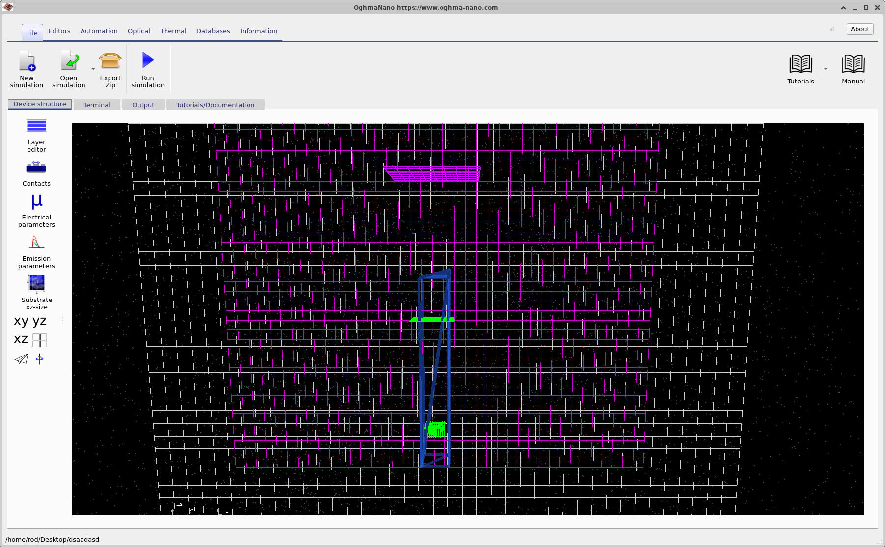
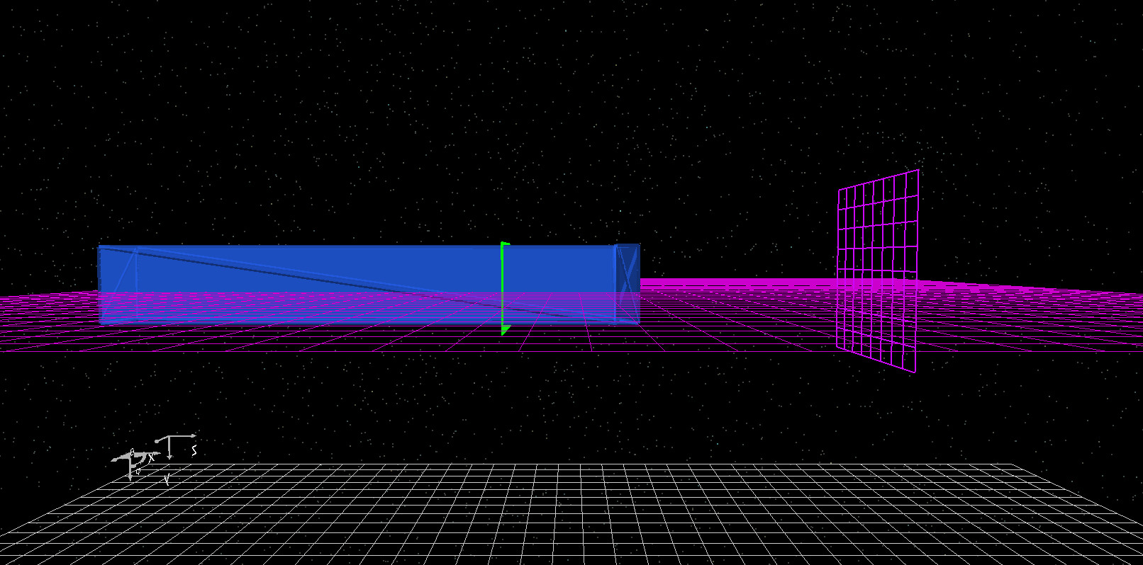
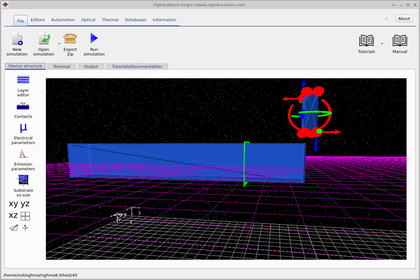
The structure is displayed in the 3D view within the Device structure tab. Two views of the same geometry are shown in ?? and ??. The blue region is the GaAs waveguide. The green plane inside the guide is the FDTD source, which launches the optical excitation. The purple plane placed some distance beyond the facet is a detector which records the transmitted signal. The example is configured so that the waveguide sits in the zx plane and the optical field is excited in the y-direction. At the output end of the guide, the structure contains a small triangular wedge of GaAs which forms the tilted facet. In the default example, this facet is shallow. Later in the tutorial we will remove it completely to make a flat facet, and then edit its geometry to create a much steeper facet. This gives us three directly comparable outcoupling structures while changing only one geometric parameter.
3. Running the simulation
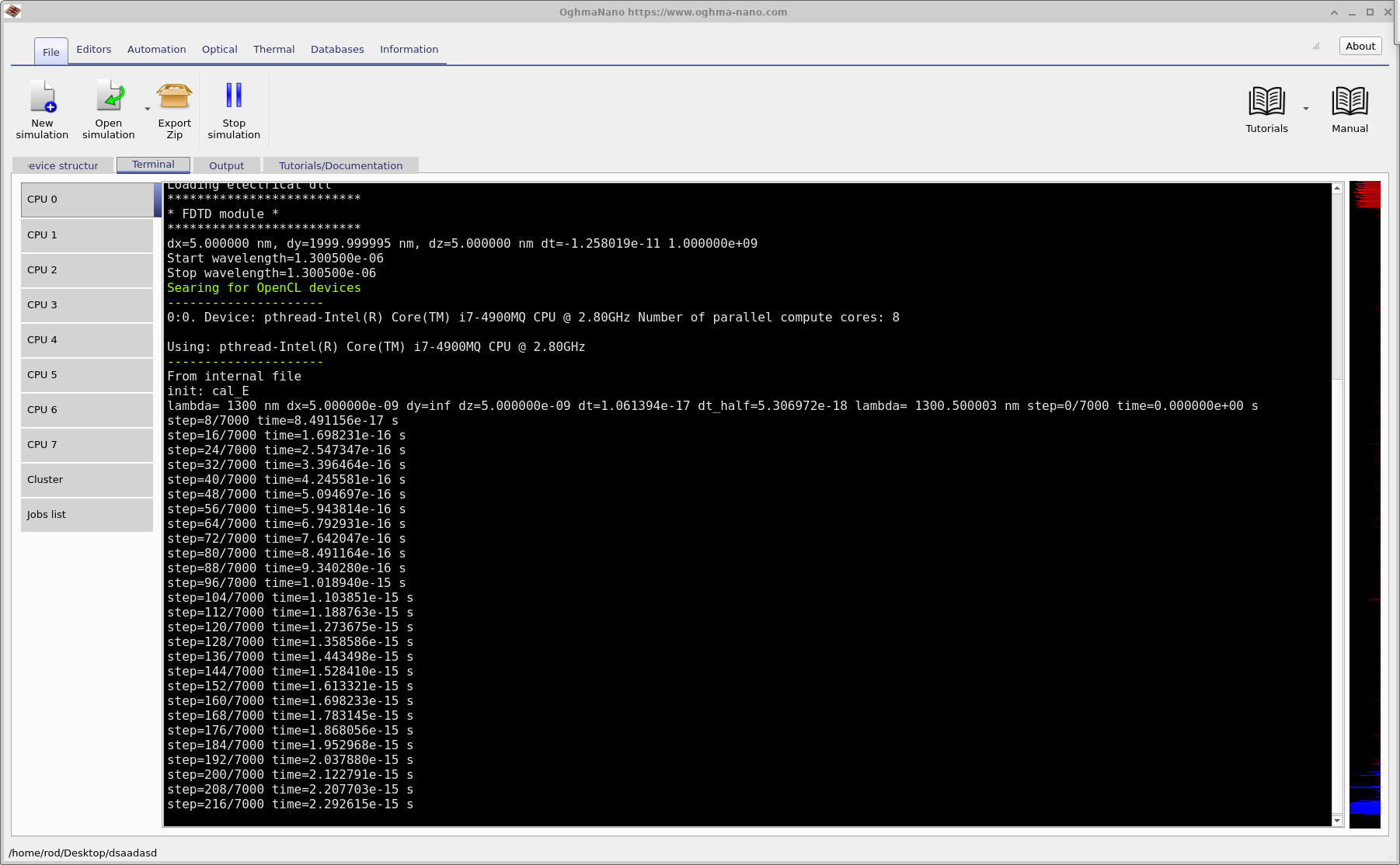
Once you have saved the simulation, click the Run (▶) button to start the calculation. As the simulation runs, you can monitor its progress in the Terminal tab, shown in
??.
This displays information such as the timestep, wavelength range, and backend being used. Near the start of the run you will see a line saying Searching for OpenCL devices. These are hardware acceleration devices that can be used to speed up the simulation. If a suitable OpenCL device is found, OghmaNano will use it automatically and run the simulation on the GPU rather than the CPU.
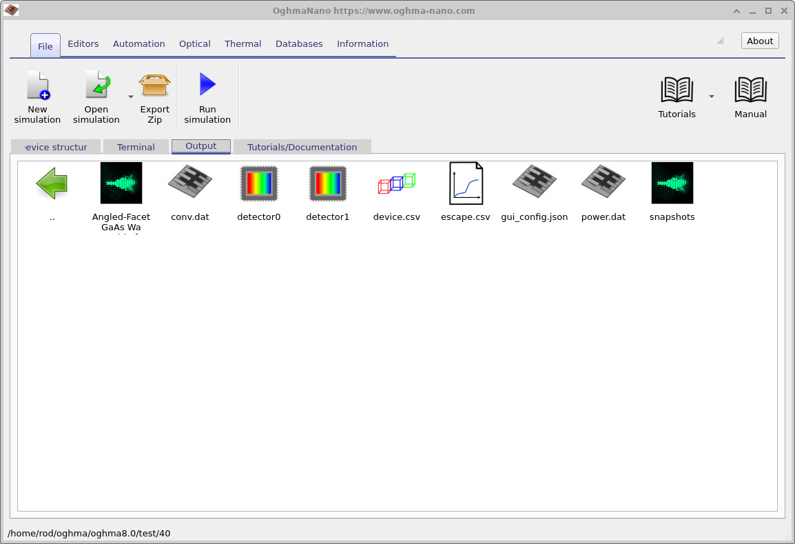
When the simulation has finished, switch to the Output tab, shown in
??.
Here you will find the data generated during the run. The most important outputs for this tutorial are the detector0 folder, which contains the transmitted spectrum, and the snapshots/ directory, which contains the time-domain field data. You should also notice that this simulation runs quickly. Because the structure is small and the example is already set up, it is well suited to quick parametric comparisons.
4. Viewing electric field snapshots
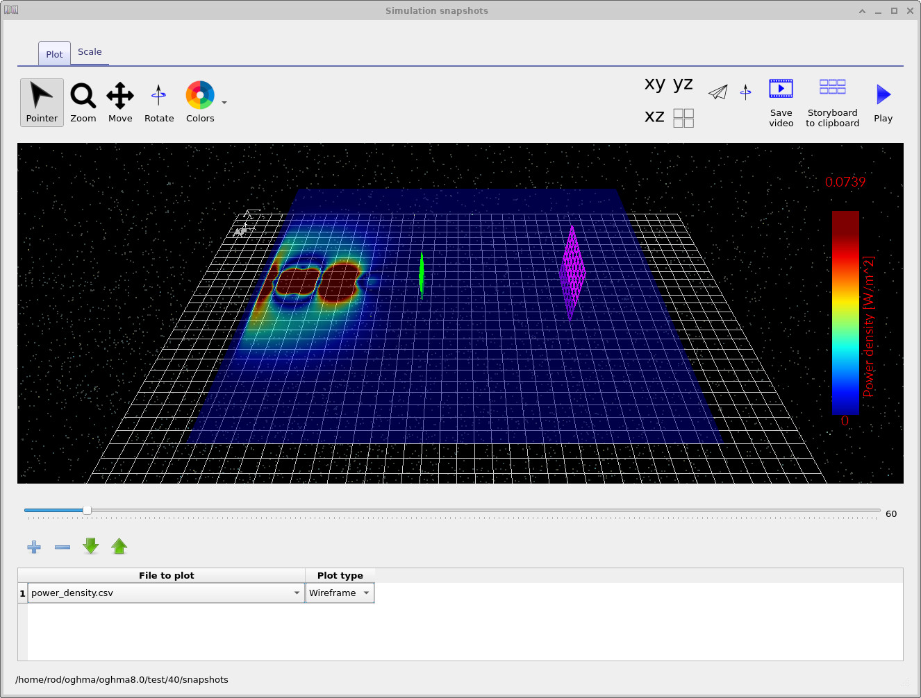
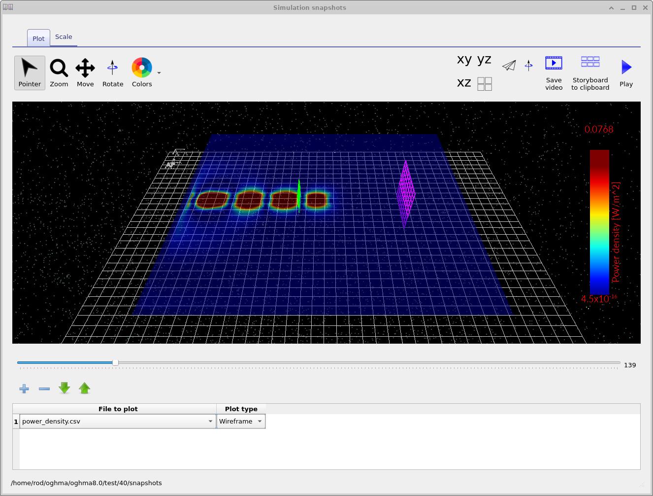
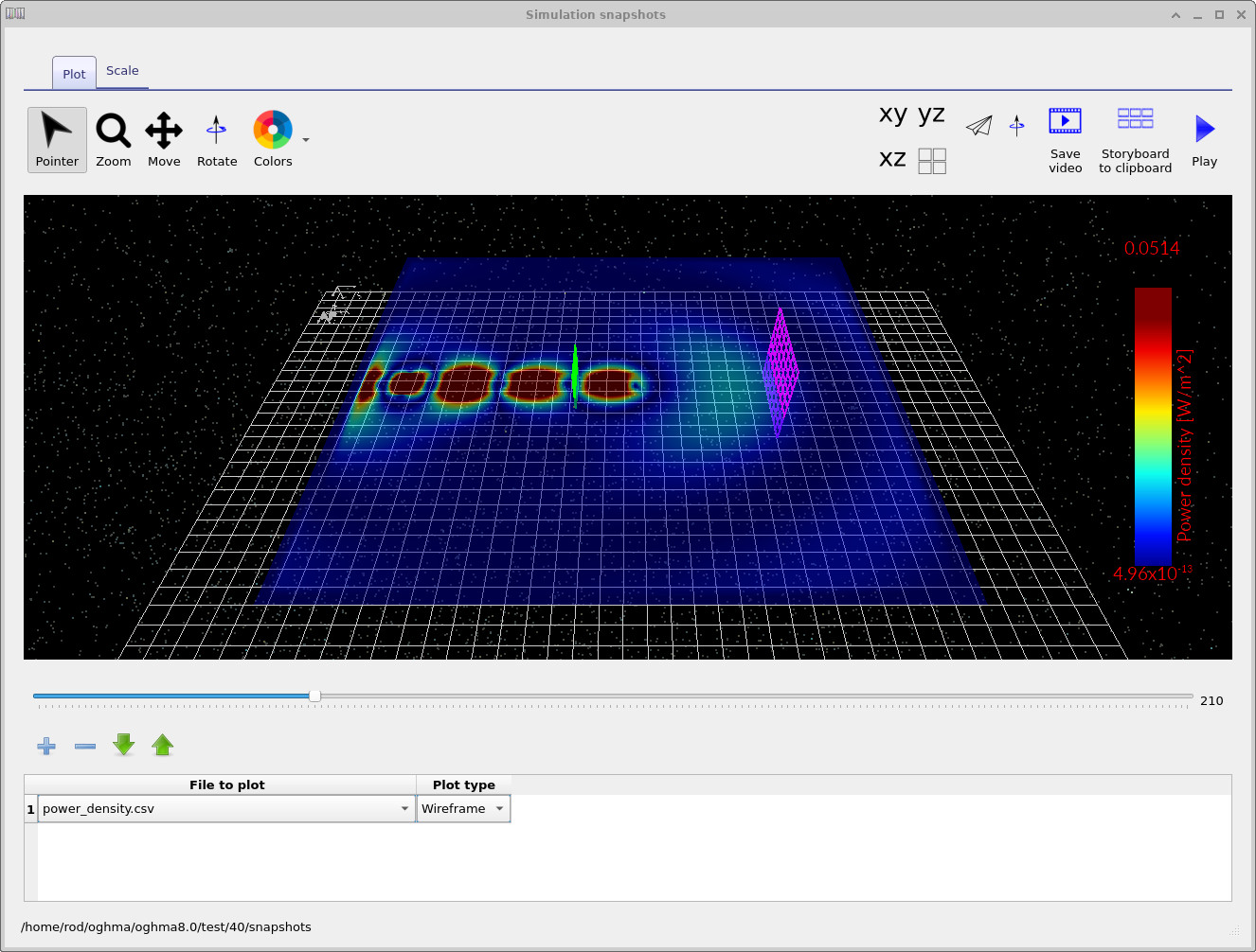
Open the snapshots/ output directory (from the Output tab) and double-click to launch the snapshot viewer. Click the + button once to add a dataset, then select the quantity you would like to view. Three representative snapshots are shown in
??–
??.
In the early-time snapshot ( ??), the guided mode is still confined inside the GaAs waveguide and is approaching the output facet. The field remains localised and strongly guided.
At intermediate times ( ??), the pulse reaches the tilted facet. The field near the output becomes asymmetric, and part of the guided mode begins to scatter into the surrounding space.
At later times ( ??), a radiated lobe is visible above the waveguide while a remaining part of the field continues to interact with the facet region. These snapshots are useful because they immediately show that the angled output is converting some of the guided mode into free-space radiation.
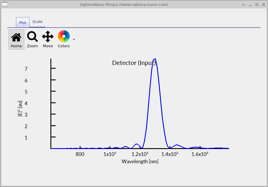
If you double-click on detector0 and select lam_E.csv, you will see the spectrum shown in
??.
A strong peak is visible at approximately 1300 nm, corresponding to the emitted optical signal from the device.
In the remainder of this tutorial, we will compare the strength of this peak as the facet geometry is changed.
5. Preparing the three comparison cases
We will now create two closely related simulations and compare the transmitted spectra recorded by detector0. Each simulation differs only in the facet geometry:
- 40 – the default shallow facet with
dx = 40 nm(≈17°) (already completed), - 130 – a steeper facet with
dx = 130 nm(≈45°), and - without – the facet moved out of the optical path, giving an effectively flat output facet.
You have already completed the 40 case. We now construct and run the remaining two so that all three geometries can be compared directly.
First, create a new simulation using the Angled Facet GaAs Waveguide for Optical Outcoupling example, exactly as described earlier, and save it with the file name without. Select the facet wedge and drag it vertically out of the optical path, as shown in
??.
In this configuration, the facet object is moved out of the FDTD simulation region so that it no longer interacts with the guided mode. The output therefore behaves as if the waveguide terminates in a flat facet.
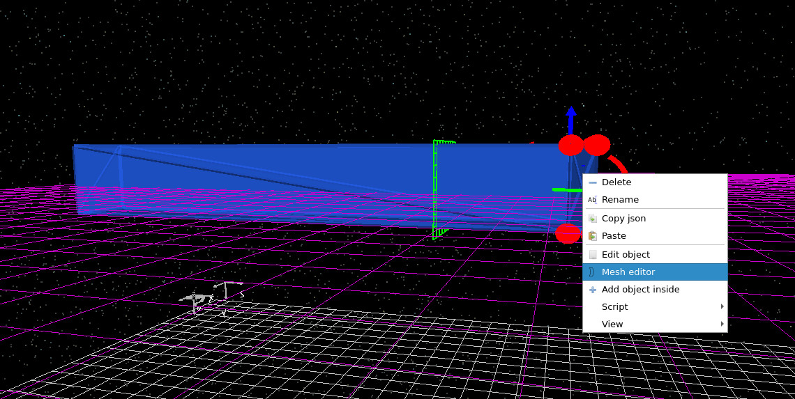
Run the without simulation and allow it to complete. Then create another new simulation using the same example (Angled Facet GaAs Waveguide for Optical Outcoupling) and save it with the file name 130. Right-click on the facet and choose Edit object, as shown in
??.
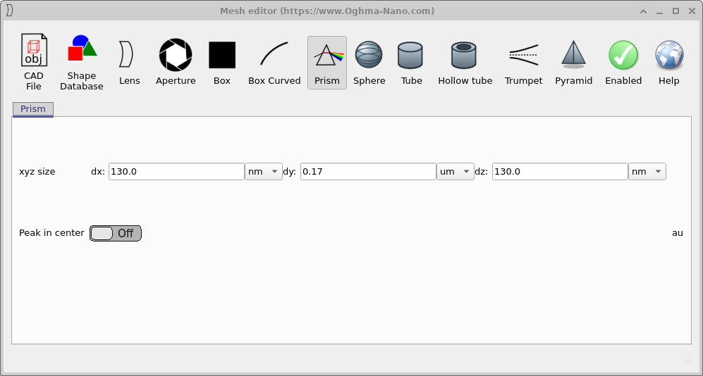
This opens the object editor shown in
??.
Change the facet dx value from 40 nm to 130 nm, apply the change, and rerun the simulation. This produces a much steeper facet, approximately corresponding to a 45° outcoupling geometry.
without case.
6. Comparing detector outputs
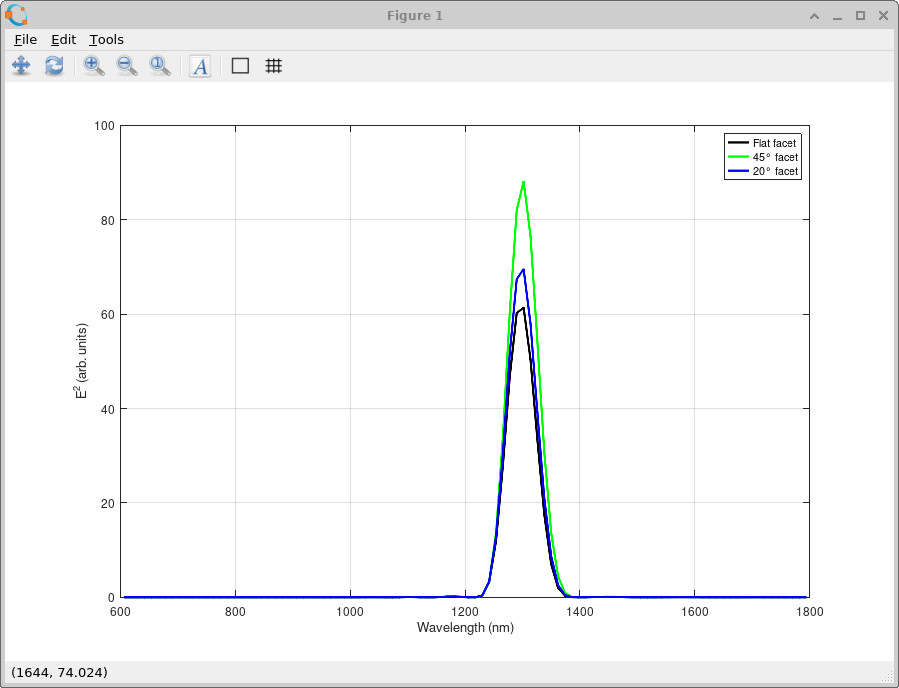
After running the three simulations, each directory will contain a file called detector0/lam_E.csv. In this tutorial, that file records the detector power spectrum as a function of wavelength. To compare the three cases, we now plot:
without/detector0/lam_E.csv130/detector0/lam_E.csv40/detector0/lam_E.csv
The final comparison is shown in ??. The horizontal axis is wavelength in nanometres, and the vertical axis is detector power in arbitrary units. This is the easiest way to compare the outcoupling behaviour of the three facet geometries.
without_data = load('without/detector0/lam_E.csv');
f130_data    = load('130/detector0/lam_E.csv');
f40_data     = load('40/detector0/lam_E.csv');

lam_without = without_data(:,1) * 1e9;   % wavelength in nm
lam_130     = f130_data(:,1) * 1e9;
lam_40      = f40_data(:,1) * 1e9;

pow_without = without_data(:,2);
pow_130     = f130_data(:,2);
pow_40      = f40_data(:,2);

plot(lam_without, pow_without, 'm', 'linewidth', 2); hold on;
plot(lam_130,     pow_130,     'g', 'linewidth', 2);
plot(lam_40,      pow_40,      'b', 'linewidth', 2);

xlabel('Wavelength (nm)');
ylabel('Power (arb. units)');
legend('Flat facet', '45° facet', '17° facet');
grid on;
import numpy as np
import matplotlib.pyplot as plt

without_data = np.loadtxt('without/detector0/lam_E.csv', delimiter=',')
f130_data    = np.loadtxt('130/detector0/lam_E.csv', delimiter=',')
f40_data     = np.loadtxt('40/detector0/lam_E.csv', delimiter=',')

lam_without = without_data[:, 0] * 1e9
lam_130     = f130_data[:, 0] * 1e9
lam_40      = f40_data[:, 0] * 1e9

pow_without = without_data[:, 1]
pow_130     = f130_data[:, 1]
pow_40      = f40_data[:, 1]

plt.plot(lam_without, pow_without, label='Flat facet')
plt.plot(lam_130,     pow_130,     label='45° facet')
plt.plot(lam_40,      pow_40,      label='17° facet')

plt.xlabel('Wavelength (nm)')
plt.ylabel('Power (arb. units)')
plt.legend()
plt.grid(True)
plt.show()
If you prefer, you can also open the three CSV files in a spreadsheet package such as Excel and plot column 1 against column 2. The only extra step is to convert wavelength from metres to nanometres by multiplying the first column by \(10^9\).
7. Physical explanation
The behaviour observed in the previous section is a direct consequence of how a guided optical mode interacts with a sudden geometric change at the end of the waveguide. Inside the GaAs waveguide, the optical field is tightly confined and propagates along the structure with a well-defined spatial profile. When this field reaches the end facet, it must reorganise itself into a form that can exist in free space. For a flat facet, this transition is inefficient. A large fraction of the optical power is reflected back into the waveguide due to the refractive index contrast, and the transmitted field expands rapidly into free space. Because the guided mode is much more confined than a free-space beam, only a limited fraction of the optical power is directed towards the detector.
Introducing a tilted facet changes this interaction. Instead of encountering a sudden, symmetric termination, the guided mode meets a sloped interface that varies along the waveguide direction. Different parts of the optical field are therefore scattered at slightly different positions, which breaks the symmetry of the reflection process and redistributes the optical power into a wider range of directions. As the facet becomes steeper, this effect becomes stronger. The sharper geometric discontinuity increases the scattering of the guided mode into radiative components, allowing more of the optical power to escape the waveguide and reach the detector. This is why the steeper facet produces a higher detected signal, even though the emitted light is less well-collimated.
The key point is that outcoupling efficiency is not determined solely by how “smooth” the emitted beam appears, but by how effectively the waveguide termination converts guided optical power into propagating radiation. In this example, the steeper facet acts as a more effective outcoupling element because it enhances this conversion process.
More detailed explanation
A more complete explanation can be given in terms of wavevectors (k-vectors). In this simulation, the waveguide runs along the z-direction, so the guided mode has a large propagation constant \(k_z\). The x-direction is across the waveguide, and the optical field is polarised in the y-direction. Inside the high-index GaAs, the magnitude of the wavevector is large, so most of the optical power is carried in components with a large \(k_z\) that remain bound to the waveguide.
To couple into free space, the field must satisfy the propagation condition in the surrounding medium. This places a limit on the allowed wavevector components: only those with sufficiently small transverse components can propagate away from the device. For a flat facet, the interface is perpendicular to the z-direction, so \(k_z\) is largely preserved. Because the guided mode has a large \(k_z\), most of the field does not satisfy the condition for propagation in free space and is therefore reflected.
A tilted facet changes this situation. The interface is no longer aligned with the coordinate axes, so the incident wavevector is effectively projected onto a new set of directions. This mixes the \(k_z\) component into \(k_x\), redistributing the wavevector components of the field. As a result, a larger fraction of the optical power falls within the range of wavevectors that can propagate in free space.
As the facet angle increases, this projection becomes stronger, enabling more efficient coupling of the guided mode into radiative components. This is why the steeper facet produces a higher detected signal, even though the emitted light is spread over a wider range of angles rather than forming a narrow beam.