FDTD tutorial: Silicon Mach–Zehnder Modulator
1. Overview: what you will simulate
A Mach–Zehnder modulator (MZM) is an interferometric photonic component that converts an electrical control signal into an optical amplitude (or intensity) change. Light is split into two waveguide arms, accumulates a relative phase difference, and is then recombined. The output power depends on the phase relation between the two arms: when the arms recombine in phase the output is bright, and when they recombine out of phase the output is suppressed.
In silicon photonics, MZMs are widely used for high-speed data communications, coherent optics, optical interconnects, and integrated microwave photonics. Practical devices typically implement phase control using electro-optic mechanisms available in the platform (for silicon this is often carrier dispersion via PN junctions, MOS capacitors, or heaters for thermo-optic tuning). Regardless of the actuation mechanism, the optical core of the device is the same: a splitter, two guided arms, and a recombiner.
In this tutorial, you will run an FDTD simulation of a representative silicon Mach–Zehnder modulator structure. The goal here is not to build a full electrical co-simulation; instead, you will use time-domain field propagation to develop intuition for how guided energy splits, travels through the two arms, and recombines at the output. You will inspect power-density snapshots and interpret detector time traces, including the propagation delay between detectors located in the arms and the detector placed further downstream where the two arms come back together.
From a numerical perspective, this example is deliberately “heavy”: the simulation domain is relatively large and it dumps a significant amount of data to disk. That makes it a good stress-test of the full FDTD stack: geometry definition, source injection, CPML absorbing boundaries, time stepping, and detector extraction, as well as the output pipeline (snapshots and detector viewers).
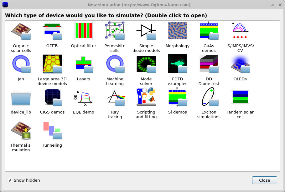
2. Making a new simulation
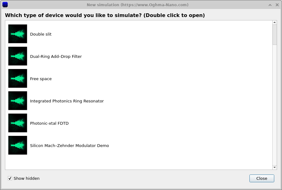
Open the New simulation window by clicking the new simulation button. In this window, select the FDTD examples category and then double-click the Silicon Mach–Zehnder modulator demo (it is listed at the bottom). When prompted, save the simulation to a local disk.
This example writes a lot of files during execution (snapshots, detector outputs, and intermediate data). For that reason, avoid saving it to a network drive or a virtualised/cloud-synced directory (for example OneDrive). A local SSD is ideal. If you save it to slow storage you may find the run time increases dramatically, or the interface becomes sluggish while writing output.
3. Orienting yourself in the main window
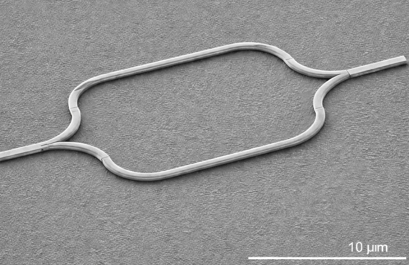
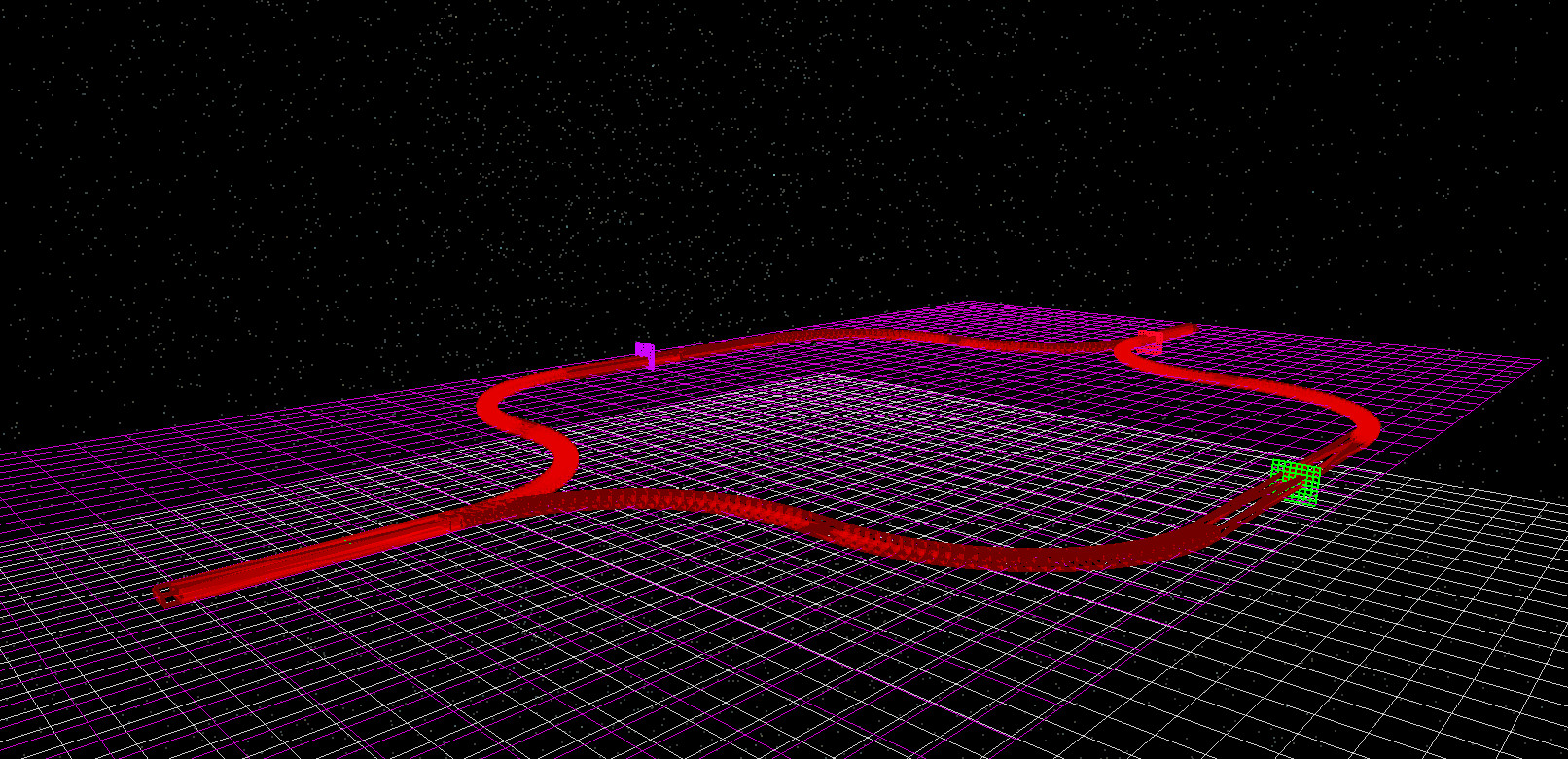
The device appears in the 3D view in the Device structure tab (??). You should be able to identify the two interferometer arms (the racetrack-like waveguide paths) and the coloured detector objects (purple, green, and red) placed along the structure. The exact colours are not important, but they make it easy to see where signals are being monitored in the geometry.
For this example you will mainly use:
- Run simulation (▶) or F9 to start the FDTD calculation.
- Output tab to open snapshots and detector directories/files.
- Snapshot viewer to step through time and observe how power density evolves.
- Detector power viewer to plot
power.csvtime traces for each detector.
4. Running the simulation
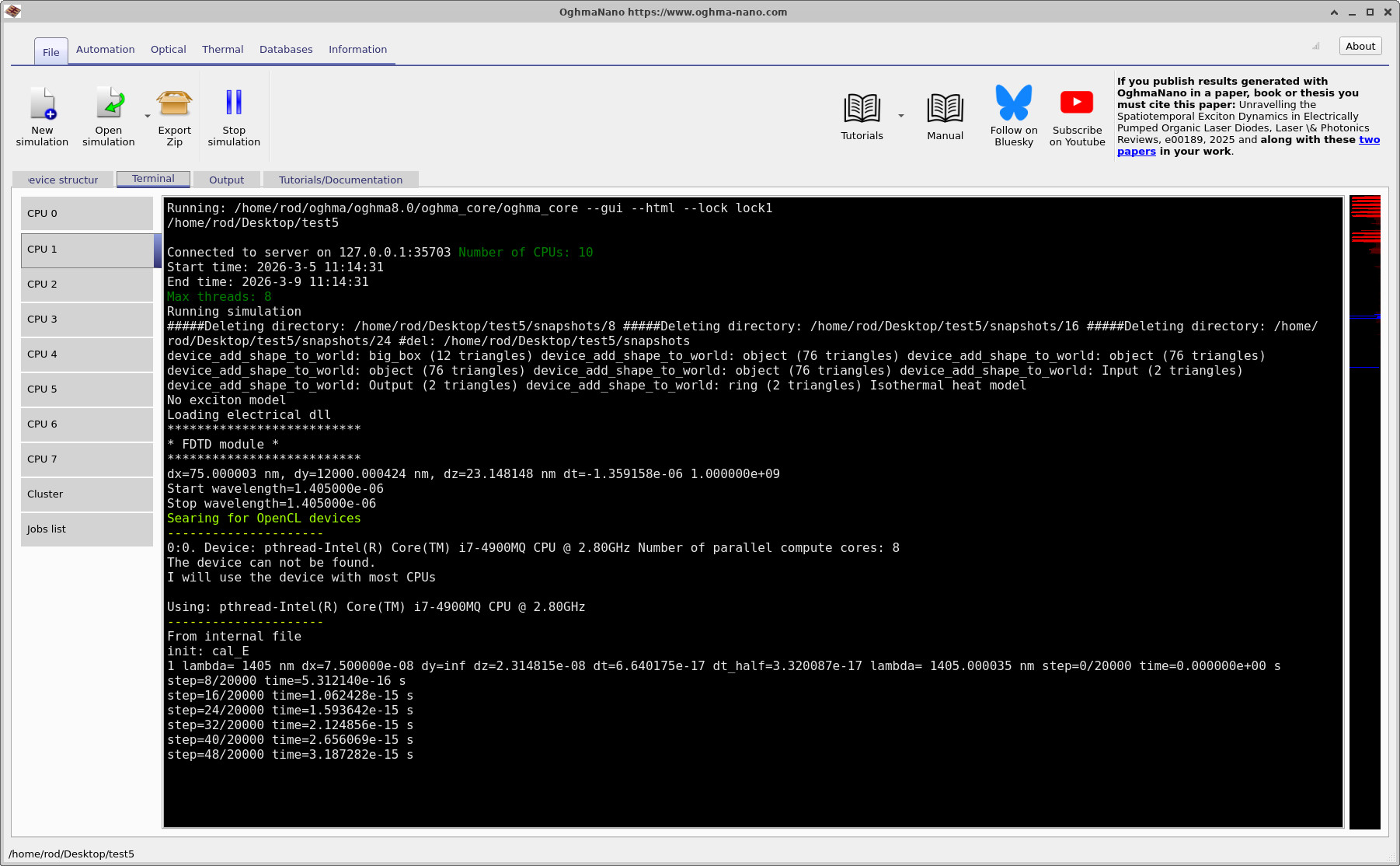
Start the run by pressing F9 or clicking the blue play button (▶). This simulation is relatively large and takes a non-trivial amount of time to complete because the grid is sizeable and because it dumps snapshots and detector data to disk.
On a reasonably powerful laptop, a typical run takes around 10–15 minutes. While the run is progressing, you
can open the Output tab and watch files appear. In particular, you will see the snapshots/ directory,
and you will see detector outputs (Detector 0, Detector 1, Detector 2) appear as the simulation advances.
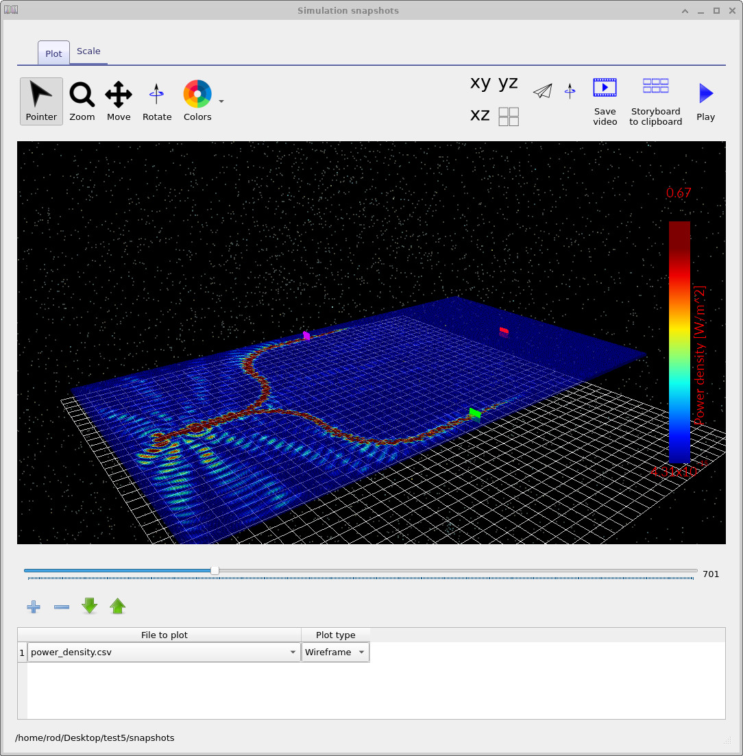
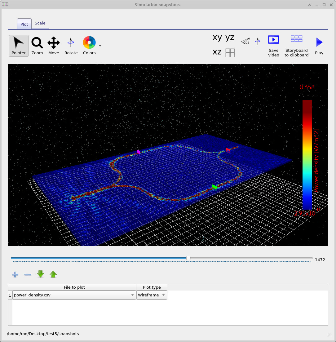
5. Viewing power density snapshots
Open the snapshots/ folder from the Output tab
(??)
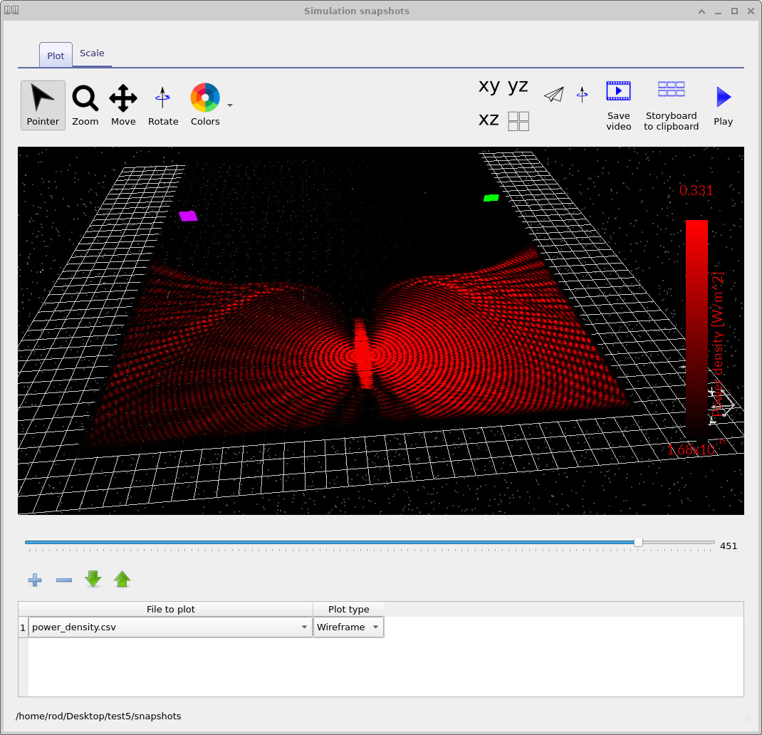
to launch the snapshot viewer. A representative snapshot-viewer window is shown in
??.
Using the blue plus button, add powerdensity.csv to the viewer. You can then step through time using the slider.
The most useful way to look at this simulation is to follow the guided energy as it propagates through the device. Early in time you will see the source launching into the input waveguide and reaching the splitter region. As time progresses, power divides between the two arms. Further snapshots show power continuing to propagate along the racetrack arms. Later still, the two arms recombine, and you can see energy routing into the output section.
Representative snapshots are shown in ??– ??. Even without changing any device parameters, these snapshots make it clear that this is an interferometric structure: energy is split, follows two physically separated paths, and then comes back together.
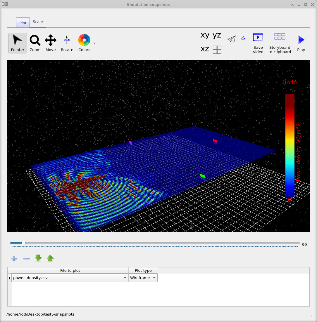
snapshots/. Add powerdensity.csv and step through time.
6. Viewing detector outputs
While the simulation runs (and after it completes), you will see detector outputs appear in the Output tab
(??).
Each detector entry looks like a small CCD-style icon. Open a detector by double-clicking it, then double-click
power.csv within that detector directory to open the detector power viewer.
This example uses three detectors. Two detectors monitor the two interferometer arms (so you can compare the time at which the guided energy reaches each arm monitor), and the third detector is positioned further downstream in the final output stage where both arms recombine. The three detector plots are shown in ??, ??, and ??.
In this run, you should observe that the power begins to ramp up at approximately \(3 \times 10^{-13}\,\mathrm{s}\) in the two arm detectors, while the downstream detector begins later (roughly about twice that time) because it is placed further along the propagation path, after the arms have travelled and recombined. This is a direct, intuitive demonstration of propagation delay through the structure: the arm monitors respond first, and the final-stage monitor responds later because the guided energy must physically travel further.
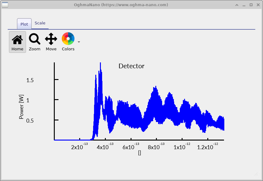
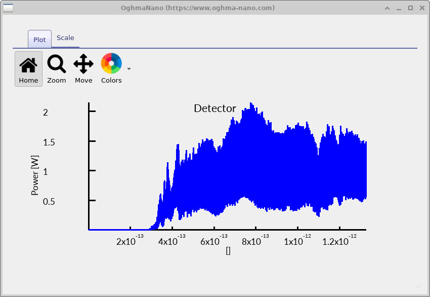
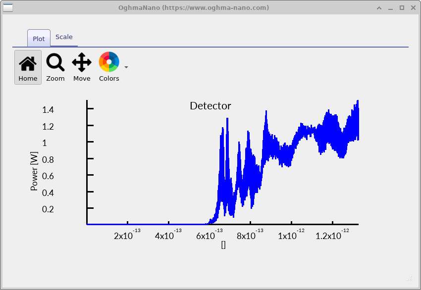
The traces are not perfectly smooth because we are not aggressively time-averaging; instead you can see the time-dependent guided content as it passes the monitors. Interpreting these plots as “instantaneous” power is not usually what you want; the more useful interpretation in this tutorial is the arrival time and the evolution of the signal envelope as the guided energy continues to propagate and interfere.
7. Inspecting the guided mode
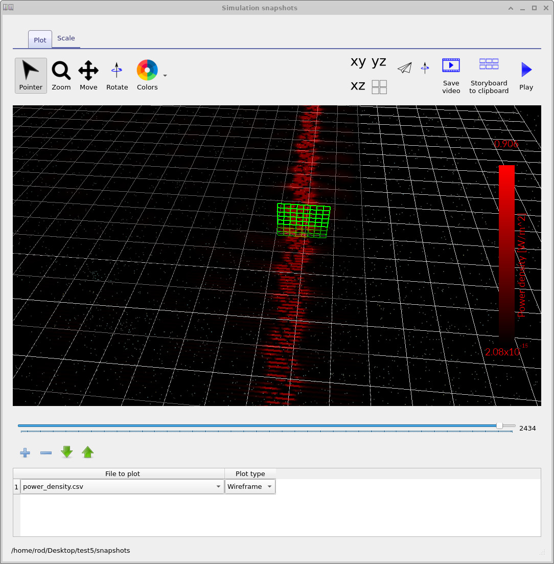
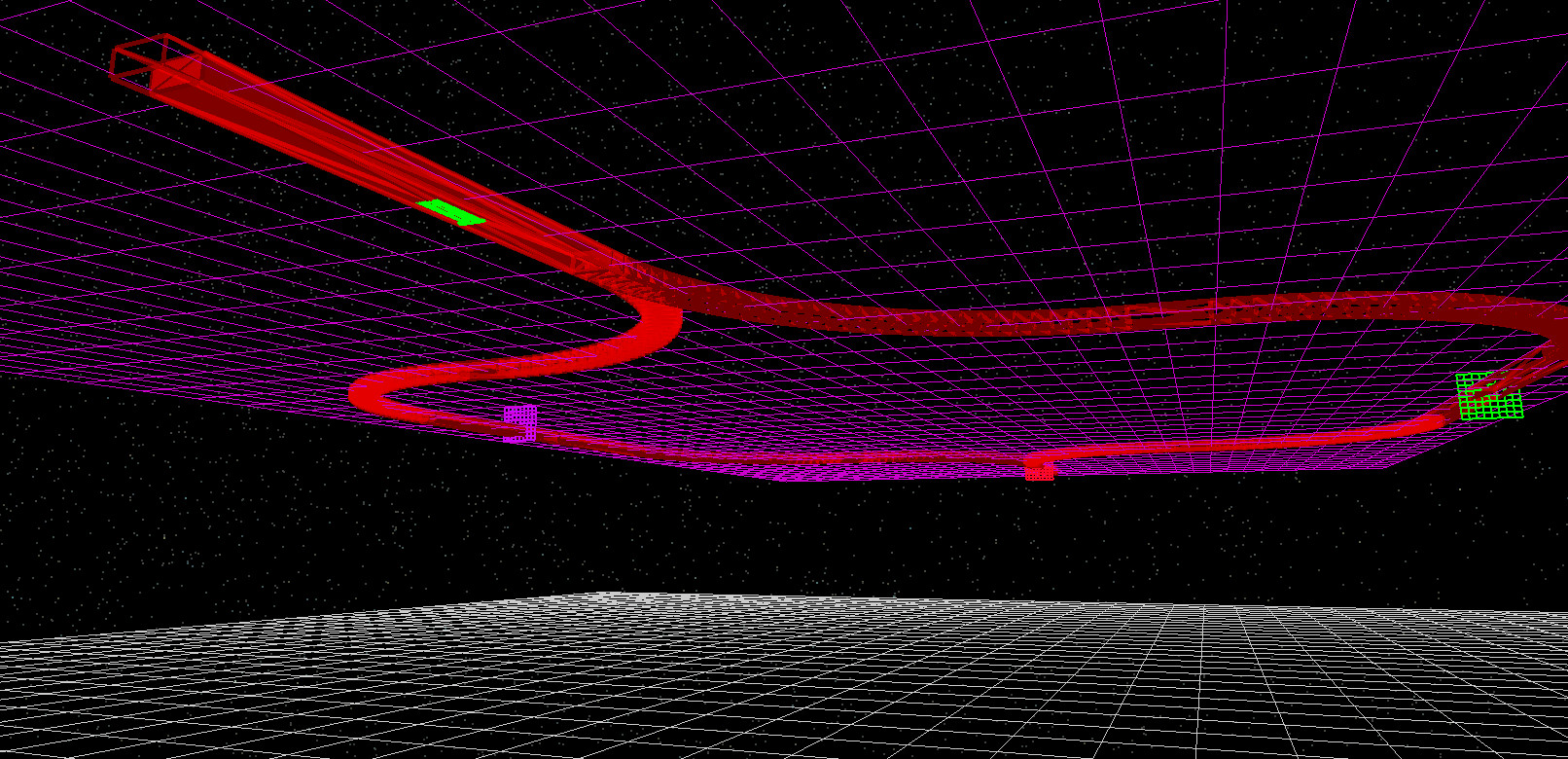
To better understand what the simulation is doing, it is useful to zoom in on the guided mode within the waveguide. An example of this is shown in ??. In this image the detector is located inside the guided mode of the waveguide.
The mode appears as a sequence of dots or short line segments. This appearance is simply an artefact of the rendering method used in the snapshot viewer: the fields are plotted as discrete sampling points to reduce GPU load and to allow large simulations to be visualised interactively. Despite this rendering style, the propagation of the guided mode is very clear and you can easily see the field travelling along the waveguide.
You can experiment with different visual styles by using the colour wheel button in the snapshot viewer toolbar. This changes the colour map used to visualise the power density field, which can sometimes make interference patterns or weak radiation features easier to see.
8. Changing the wavelength of the excitation
The behaviour of photonic structures such as Mach–Zehnder interferometers depends strongly on the wavelength of the injected light. In the example provided with OghmaNano the wavelength is chosen to match the guided mode of the silicon waveguide. As an experiment we will now deliberately change the wavelength so that the structure no longer supports guided propagation.
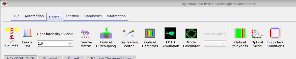
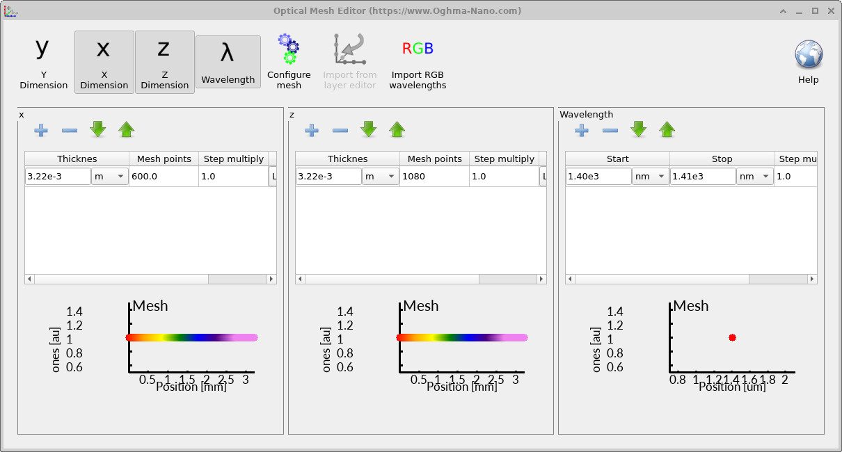
Navigate to the Optical ribbon shown in ?? and open the optical mesh editor. In the wavelength settings (??) change the wavelength range so that the simulation runs at green light.
Set the start wavelength to 530 nm and the stop wavelength to 531 nm. This is far shorter than the wavelength originally used in the example.
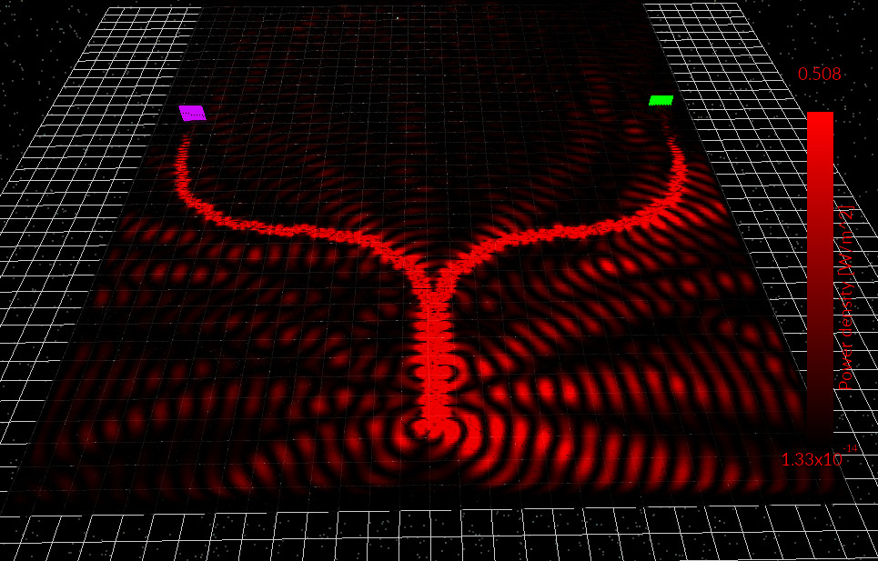
After making this change, rerun the simulation. The result is shown in ??. Instead of remaining confined to the waveguide, the optical field now spreads outward into the simulation domain. The result is a striking radiation pattern that resembles a butterfly or interference fan.
This occurs because the wavelength is now much smaller relative to the waveguide geometry, so the structure no longer supports a well-confined guided mode. The Mach–Zehnder interferometer therefore stops behaving like a photonic circuit and instead behaves more like a simple radiating aperture.
This experiment highlights an important design principle in integrated photonics: waveguide structures are highly wavelength dependent. You can repeat this test with different wavelengths to determine which spectral regions support guided propagation within this geometry.
9. Mesh resolution and radiating modes
In the default example you will notice that the waveguide bends appear extremely smooth. This is intentional. Smooth bends help to keep the optical mode confined inside the waveguide and prevent radiation losses when the optical field changes direction.
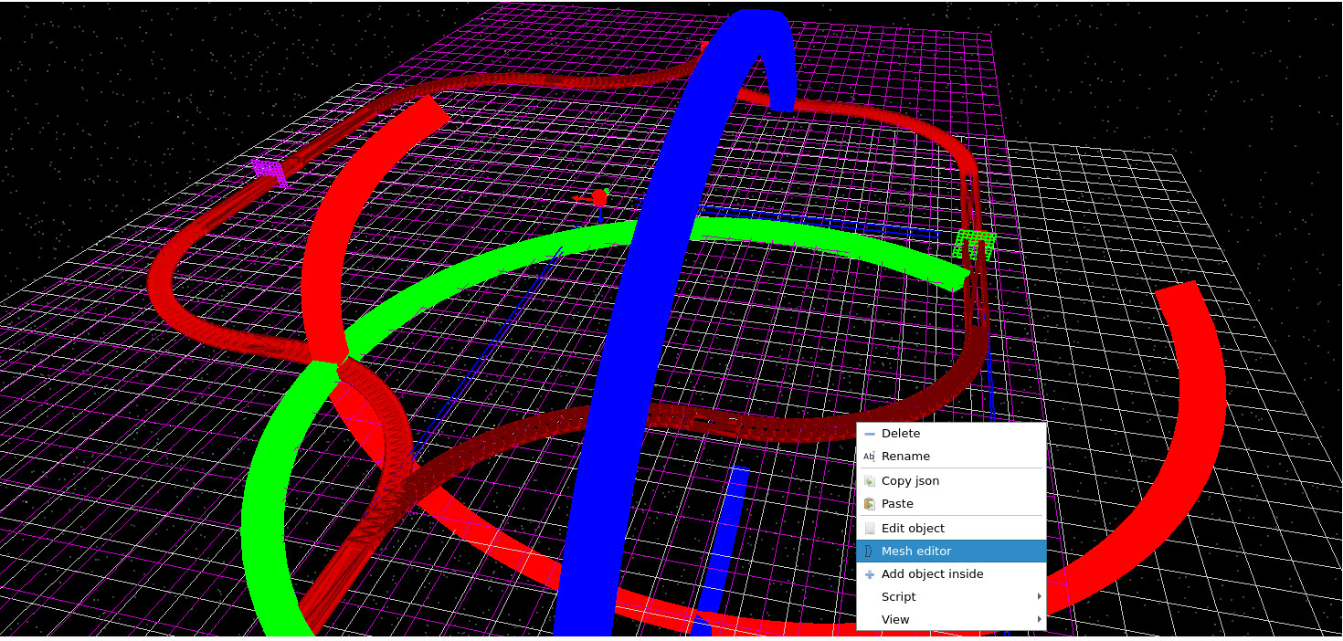
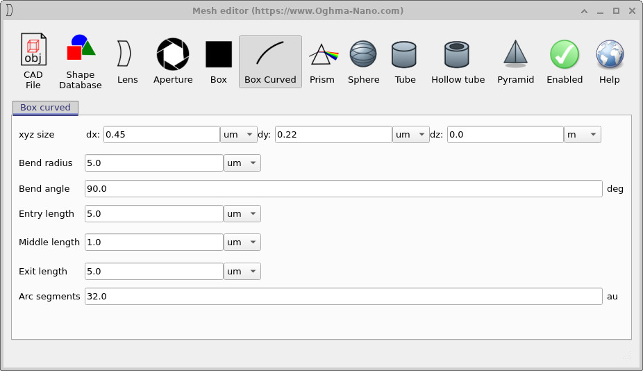
The Mach–Zehnder structure in this tutorial is constructed from four curved waveguide segments forming a racetrack-shaped interferometer. To demonstrate the importance of smooth geometry, right-click the curved waveguide element closest to you and select Mesh editor (??).
This opens the mesh editor window shown in ??. Locate the parameter called Arc segments. In the original example this value is set to 32, which produces a smooth curved waveguide.
Reduce the number of arc segments to 1. This is the smallest number of segments allowed and effectively converts the smooth bend into a crude polygon constructed from rectangular sections.
When you rerun the simulation you will observe strong radiation losses around the corners of the waveguide, as shown in ??. As the optical field reaches each sharp change in direction, part of the energy is no longer guided and escapes as radiation.
You will also see some radiation near the source injection region. This radiation is simply caused by a mismatch between the injected source eigenmode and the exact eigenmode of the waveguide and can be ignored for this demonstration.
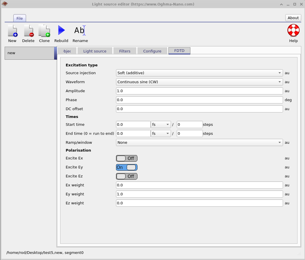
10. Editing the light source
Finally, we will briefly explore how the excitation source can be modified. By default the simulation uses a continuous sine-wave source. However, OghmaNano allows a wide range of source types and parameters to be configured.
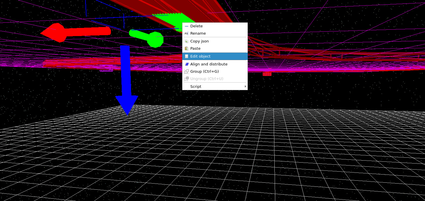
Switching to the view shown in ?? reveals the excitation source as a green arrow emerging from the bottom of the waveguide. Right-click this arrow and select Edit object (??).
This opens the light source editor (??), which allows you to configure the excitation waveform. Instead of a continuous sine wave you can specify pulses, change the start and stop times, or excite different field components.
A useful experiment is to set the source duration in terms of simulation steps rather than femtoseconds. For example, set the end time to approximately 400 steps. When the simulation runs, the source will inject a burst of light into the waveguide and then switch off. You can then watch the resulting wave packet propagate through the interferometer and eventually leave the structure.
You can also experiment with exciting different field components (x, y, or z polarisation) or testing different pulse shapes. These variations are extremely useful when studying transient behaviour, group delay, or pulse distortion in photonic devices.
This concludes the Mach–Zehnder modulator tutorial. By experimenting with wavelength, mesh resolution, and source parameters you can explore how photonic structures guide, confine, and manipulate optical fields in integrated photonic circuits.