Anti-Reflective Coating Simulation (FDTD): 1D Thin-Film Tutorial
1. Introduction
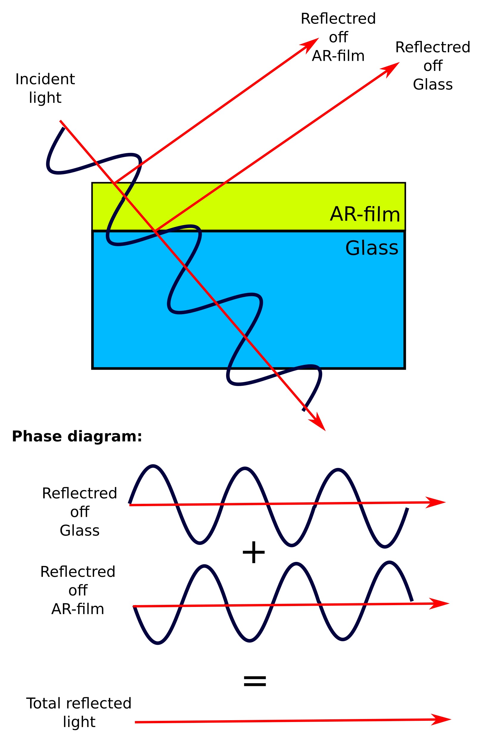

Whenever light encounters a boundary between two materials with different refractive indices, some of the light is transmitted and some is reflected. This is why bare glass surfaces often appear shiny, even when the glass itself is transparent. An anti-reflective (AR) coating is a thin optical film designed to reduce this unwanted reflection and thereby increase the transmitted light.
The basic idea is shown in ??. Rather than trying to eliminate reflection at a single interface, we add a thin intermediate layer between air and the substrate. Light now reflects from two places: the air–film interface and the film–substrate interface. If the film is chosen correctly, these two reflected waves have similar amplitudes but opposite phase, so they interfere destructively. The result is that the net reflected field is strongly reduced.
Phase matching: To cancel reflection, the two reflected waves must return half a wavelength out of step (a phase difference of \(\pi\)). We usually design this for light incident normal to the surface, even though ?? shows the geometry at an angle for clarity.
The first reflection occurs at the air–film surface. The second reflection comes from the film–substrate interface, but this wave has travelled down through the film and back again. If the film thickness is \(d\), this extra distance is \(2d\).
Inside the film, light travels more slowly, so the wavelength is reduced by the refractive index \(n_f\). This means the extra optical path length is \(2n_f d\). For destructive interference, this must equal half a wavelength:
\(2n_f d = \dfrac{\lambda_0}{2}\)
which gives
\(d = \dfrac{\lambda_0}{4n_f}\)
So the coating thickness \(d\) is chosen to be one quarter of the wavelength (inside the film), ensuring the lower reflected wave returns half a wavelength out of phase with the upper one and cancels it.
Amplitude matching: Phase cancellation alone is not sufficient; the two reflected waves must also have similar amplitudes. For a non-absorbing single-layer coating at normal incidence, this is achieved when the coating refractive index is approximately
\(n_f \approx \sqrt{n_0 n_s}\)
where \(n_0\) is the refractive index of the incident medium and \(n_s\) is that of the substrate. For air on glass, this gives an ideal index around 1.2–1.3, which is lower than most practical materials. As a result, real coatings are typically approximate, or use multi-layer designs to improve performance.
The practical effect is shown in ??: the reflected glare is reduced and the substrate appears more transparent. This principle is widely used in solar cells, lenses, and optical coatings.
In this tutorial, we use the Finite-Difference Time-Domain (FDTD) method to simulate a simple 1D anti-reflective coating. By running the model, you will see how the coating modifies reflection and transmission, and how the film thickness sets the wavelength at which reflection is minimised.
2. Making a new simulation
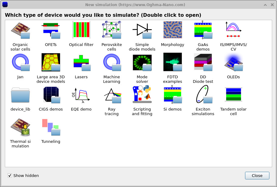
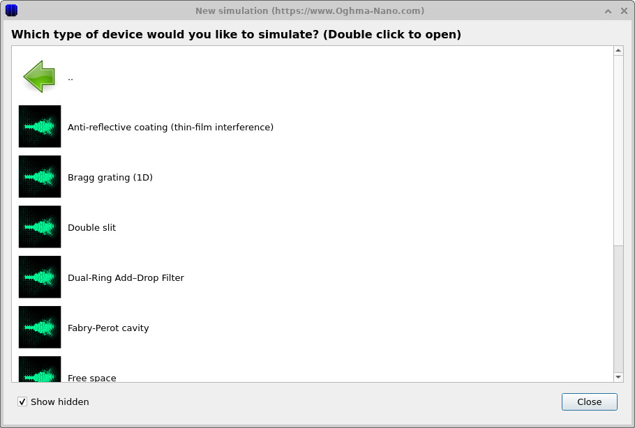
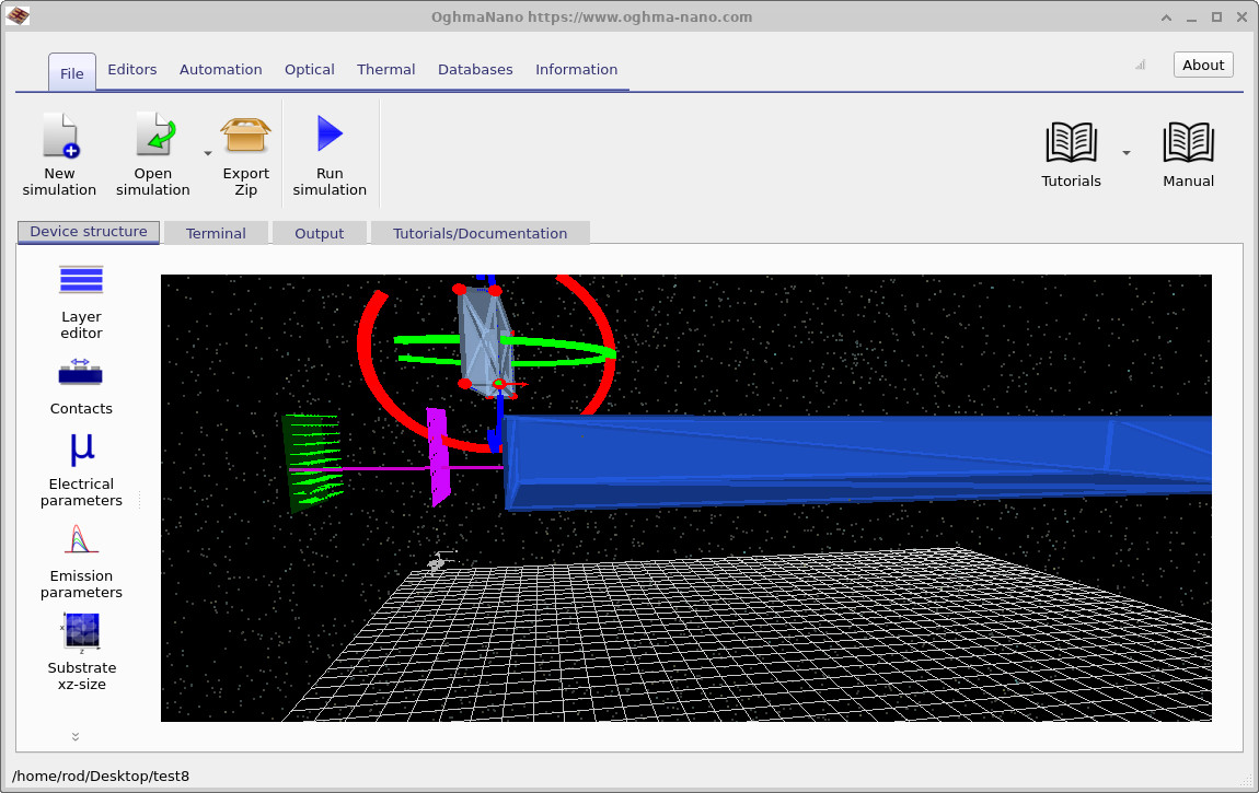
Open the New simulation window and select the FDTD examples category (??). Then choose the Anti-reflective coating (think film interference) example (??). This loads the main interface shown in ??.
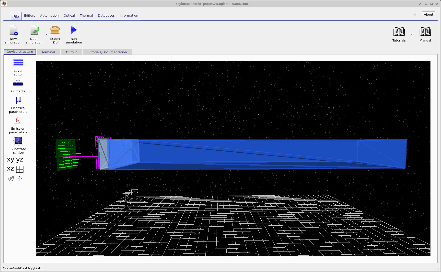
The structure is displayed in the 3D view within the Device structure tab. This view shows all the key components of the anti-reflective coating simulation. On the left, the green arrows represent the FDTD source, where the optical pulse is injected. The thin purple line running through the structure is the FDTD grid. In this example, the simulation is effectively one-dimensional, so the grid appears as a single line passing through the coating and substrate.
Just to the right of the source, the purple plane represents a detector, which records the incident and reflected fields. It does not influence the simulation, but simply samples the electromagnetic field across the grid. Further to the right is the thin anti-reflective coating deposited on the substrate. The light blue region corresponds to this coating layer, while the much thicker region represents the gallium arsenide (GaAs) substrate. In this example, we use GaAs rather than glass, as this type of coating is commonly applied to devices such as photodetectors to improve light coupling.
3. Running the simulation
Once you have saved the simulation and had a look around the structure, click the Run (▶) button to start the calculation.
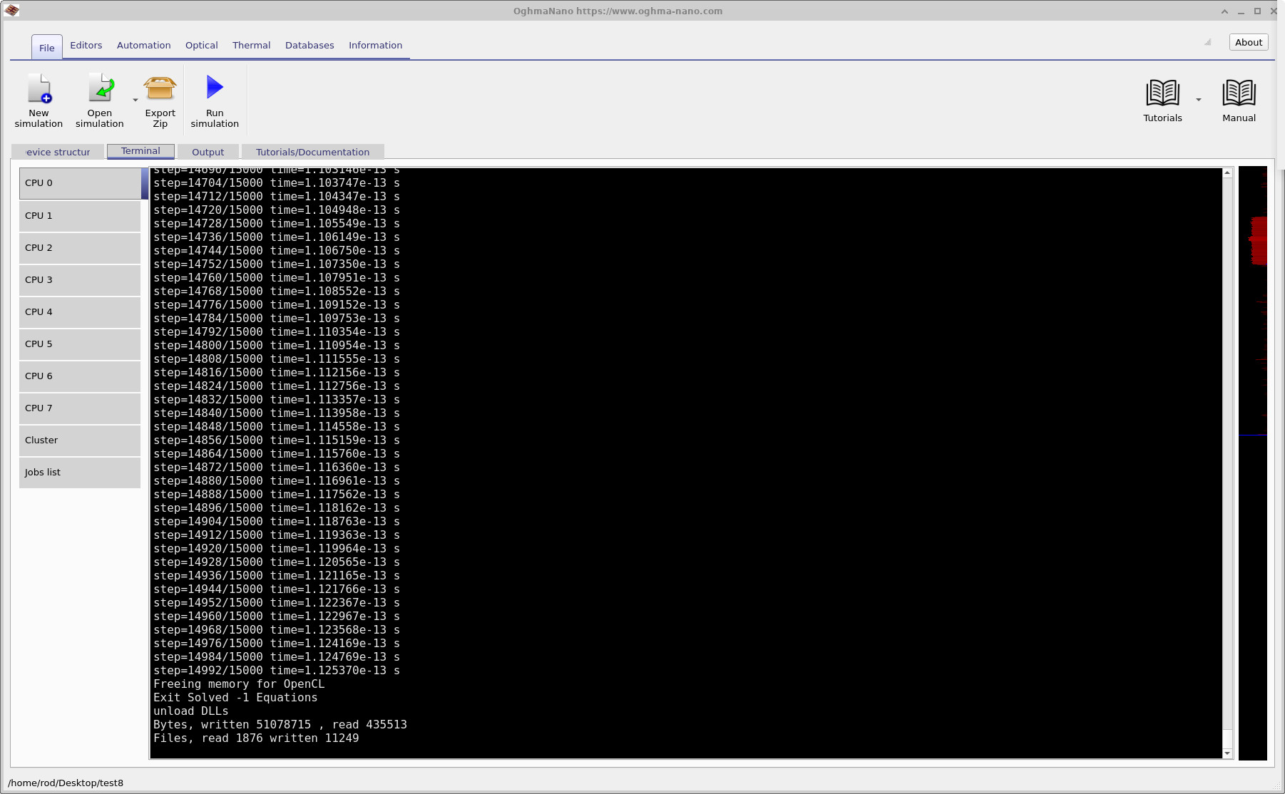
As the simulation runs, you can monitor its progress in the Terminal tab, shown in
??.
This displays information such as the timestep, wavelength range, and backend being used. Near the start of the run you will see a line saying Searching for OpenCL devices. These are hardware acceleration devices that can be used to speed up the simulation. If a suitable OpenCL device is found, as in the example shown in the figure, OghmaNano will use it automatically and run the simulation on the GPU rather than the CPU.
When the simulation has finished, switch to the Output tab, shown in
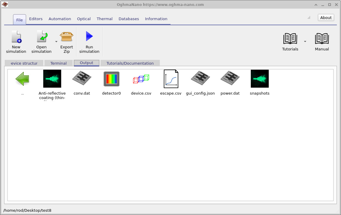
??.
Here you will find the data generated during the run. The key outputs for this tutorial are detector_0 and detector_1, which contain the signals recorded by the two detectors.
You can also open device to view the 3D geometry, and the snapshots/ directory to see how the electromagnetic fields evolve over time.
You should notice that this simulation runs very quickly. Because it is a 1D problem, typical run times are only a few seconds.
If the simulation is taking significantly longer than this, refer to the note above about saving the simulation on a fast local drive.
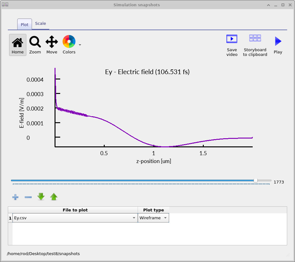
5. Viewing electric field snapshots
Open the snapshots/ output directory (from the Output tab) and double-click to launch the snapshot viewer.
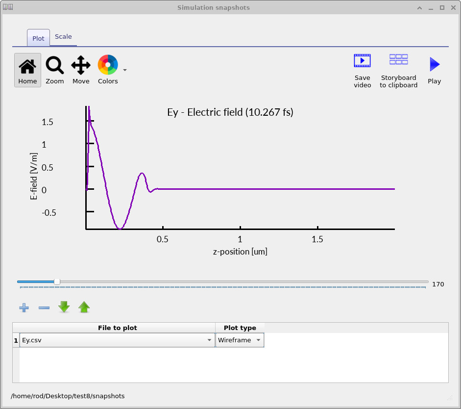
This allows you to view the simulation results as a function of time. Click the + button once to add a dataset, then select Ey. In this simulation the field is excited in the
y-direction, so this component gives the most direct view of the wave propagation.
You can then use the slider bar to step through time and observe how the field evolves. Three representative snapshots are shown in
??–
??.
At early times (left panel, ??), you can see the initial broadband pulse travelling toward the coated surface. The field is still spatially localised, with a sharp leading edge corresponding to the injected excitation.
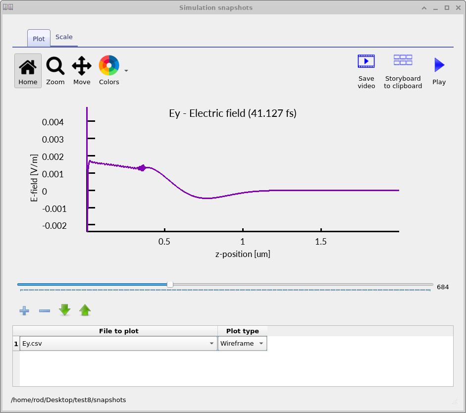
As time progresses (middle panel, ??), the pulse reaches the thin film and substrate. Part of the wave is reflected while part is transmitted. The field near the interface shows small oscillations due to partial reflection and the broadband nature of the pulse, rather than a single-frequency interference pattern.
At later times (right panel, ??), the forward-propagating transmitted wave dominates inside the substrate, while a weaker reflected component travels back toward the source. In a well-designed anti-reflective structure, this reflected component is smaller than it would be for an uncoated interface. This reduction does not arise because reflection disappears at each interface individually, but because the reflected contributions combine destructively.
6. Viewing detector outputs
Returning to the Output tab (see
??),
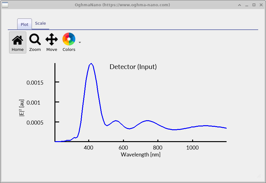
you will see a folder labelled Detector0. In this example, only a single detector is used,
positioned on the source side of the structure to measure the incoming and reflected light. Open Detector0 and locate the file lam_E.csv. This file contains the frequency-domain
response of the electric field at the detector. Double-click it to plot the spectrum, as shown in
??.
You should observe a strong peak centred near the main wavelength of the source (around 400 nm). The magnitude of this peak is relatively small (of order \(10^{-3}\)–\(10^{-2}\)), indicating that only a limited fraction of the light is being reflected back toward the detector. This is the effect of the anti-reflective coating. To confirm this, return to the Device structure tab and move the coating out of the optical path. As shown in ??, click on the coating and drag it away from the main propagation direction using the left mouse button. If the object becomes difficult to move due to overlap, use the arrow keys (with Shift) to reposition it slightly until it is free.
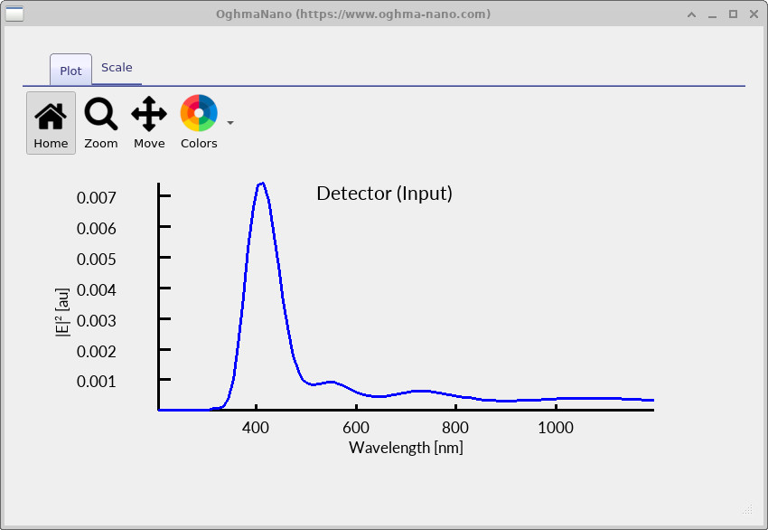
Once the coating has been removed from the path, rerun the simulation. Then return to Detector0
and open lam_E.csv again. The result is shown in
??. You should now observe a much larger peak at the source wavelength. This indicates that a significantly greater fraction of the light is being reflected at the interface when the coating is absent.
It is important to note that this detector primarily measures light passing through it from the source direction. When the coating is present, destructive interference reduces the reflected component, so the detected signal is relatively small. When the coating is removed, reflection increases, and more light is redirected back toward the detector, leading to the larger peak.
This comparison clearly demonstrates the function of the anti-reflective coating: it reduces the reflected light at the design wavelength, allowing more of the incident light to enter the substrate.
7. Comparing spectra with and without the anti-reflective coating (optional)
In FDTD simulations, it is often very useful to compare results before and after making a change to the structure. In this case, we compare the response of the device with and without the anti-reflective coating. This step is not required to complete the tutorial, but if you have access to a tool such as MATLAB or Octave, it provides a much clearer view of the coating performance.
The reason for doing this comparison is that the raw detector signal is strongly influenced by the spectral shape of the source.
By comparing two simulations with the same source, this influence largely cancels out, allowing you to isolate the effect of the coating itself. First, run the simulation without the coating (as described in the previous section).
Then open the Detector0 folder and copy the file lam_E.csv to a new file, for example without.csv.
Next, return to the device structure, move the coating back into the optical path, and rerun the simulation.
Once the run is complete, again copy lam_E.csv, this time saving it as with.csv.
You now have two datasets: one for the uncoated structure and one for the coated structure.
These can be compared directly using MATLAB or Octave with the following script:
with_data    = load('with.csv');
without_data = load('without.csv');

lam_m = without_data(:,1);          % wavelength in meters
lam   = lam_m * 1e9;               % convert to nanometers

ref0 = without_data(:,2);
ref1 = interp1(with_data(:,1), with_data(:,2), lam_m, 'linear');

ratio = ref1 ./ ref0;

plot(lam, ratio, 'k', 'linewidth', 2);
xlabel('Wavelength (nm)');
ylabel('Relative reflection');
title('Anti-reflective coating response');
grid on;
ylim([0 1.2]);
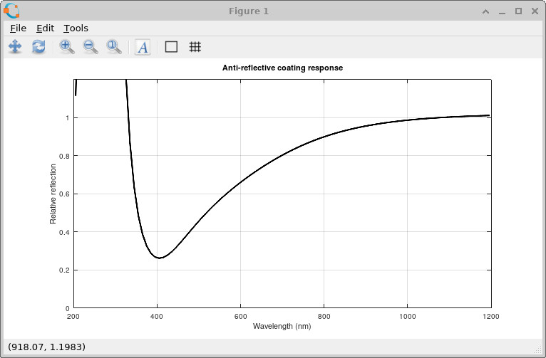
The resulting plot is shown in ??. You should observe a clear dip in the relative reflection around 400 nm. This dip corresponds to the design wavelength of the anti-reflective coating. At this wavelength, the reflected waves from the two interfaces cancel, reducing the net reflected light. Away from this wavelength, the phase condition is no longer satisfied, and the reflection gradually increases again. This comparison provides a clear, quantitative demonstration of how the coating modifies the optical response, and is often the easiest way to evaluate thin-film designs in practice.
8. Try it yourself
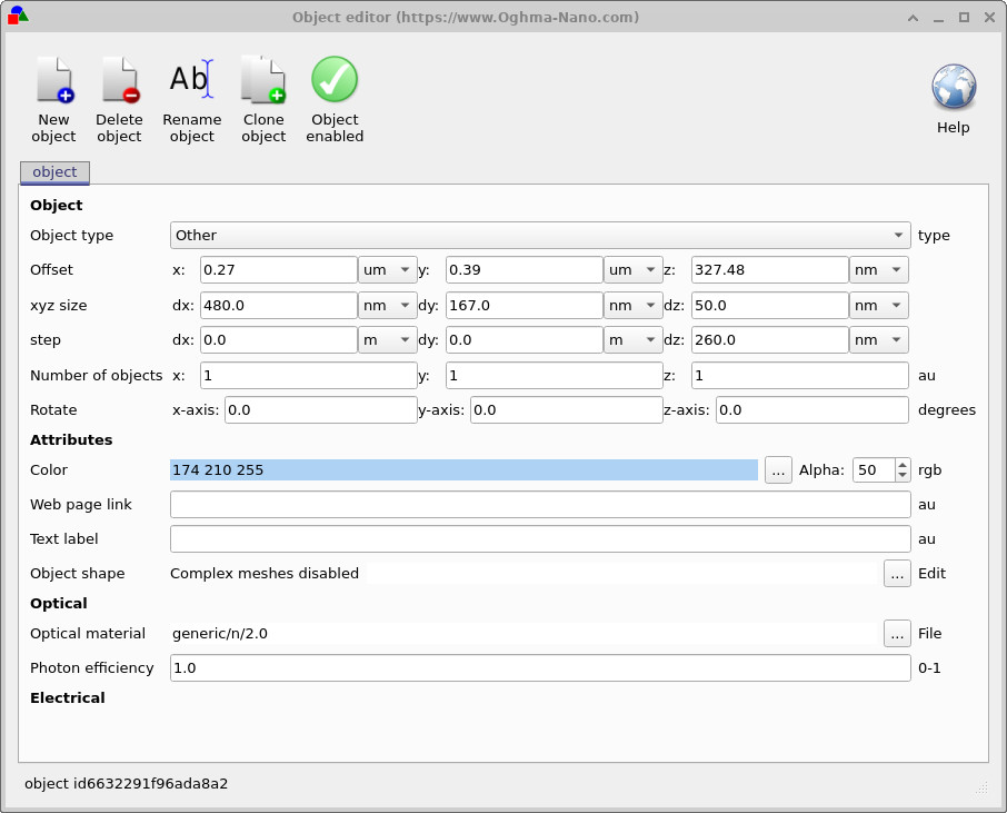
To get a better feel for how the coating works, try modifying its thickness. Right-click on the coating and select Edit object (see ??), then change the Dz value from 50 nm to 60 nm and 70 nm.
After each change, rerun the simulation and inspect the detector output. The effect may be subtle in the raw data, so it is helpful to compare the spectra using the MATLAB/Octave method described in the previous section.