Bifacial Perovskite Solar Cell Simulation Tutorial: Dual-Side Illumination and Optical Analysis in OghmaNano

1. What is a bifacial perovskite solar cell?
A bifacial solar cell is a photovoltaic device designed to absorb light incident on both its front and rear surfaces simultaneously ( ??). In a conventional (monofacial) solar cell, only the top surface is illuminated; the rear contact is typically opaque, so any light reaching the back of the device is lost. In a bifacial architecture, both contacts are made transparent or semi-transparent - for example, using ITO (indium tin oxide) or FTO (fluorine-doped tin oxide) - allowing the rear surface to collect reflected, scattered, or diffuse irradiance from the surroundings.
For perovskite solar cells (PSCs), bifacial operation is particularly attractive because:
- The perovskite absorber layer (e.g. MAPbI₃) has a very high absorption coefficient, meaning it can harvest photons efficiently even when they arrive from below.
- Both charge-transport layers (TiO₂ as the electron transport layer and Spiro-OMeTAD as the hole transport layer) can be made sufficiently thin and transparent not to block rear-side illumination significantly.
- In real-world field conditions - particularly in bifacial module installations with a white or reflective albedo surface - rear-side irradiance can add 5–30% additional power output compared with monofacial operation.
The bifaciality factor ηbif is defined as the ratio of the rear-side efficiency to the front-side efficiency:
\[ \eta_{\text{bif}} = \frac{\eta_{\text{rear}}}{\eta_{\text{front}}} \]
A perfect bifacial device would have ηbif = 1, meaning it performs equally well under illumination from either side. In practice, values between 0.7 and 0.95 are common for perovskite bifacial cells, depending on the asymmetry of the charge-transport layers and the transparency of each contact.
In OghmaNano, bifacial operation is modelled by adding two independent light source objects - one illuminating from the top (y0) and one from the bottom (y1) - and coupling both into the optical transfer matrix solver. This tutorial walks through the complete workflow, from loading the template simulation to analysing the resulting optical fields and JV characteristics.
2. Create a new bifacial perovskite simulation
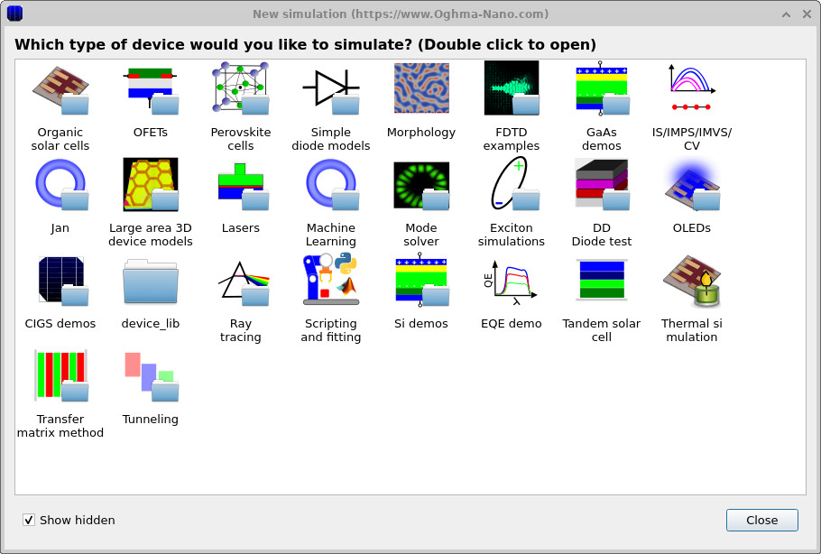
Start OghmaNano from the Windows and select New simulation. This opens the device library shown in ??. Double-click Perovskite cells to open the perovskite examples folder. You will then see the list of available perovskite templates shown in ??. Double-click Perovskite Bifacial Solar Cell (MAPI) to load the bifacial example. When prompted, choose a destination folder on a local drive and click Save.
💡 Tip: Save to a local drive such as C:\. Simulations stored on
network shares, USB drives, or cloud-synced folders (e.g. OneDrive, Dropbox) can run
slowly due to frequent read/write operations.

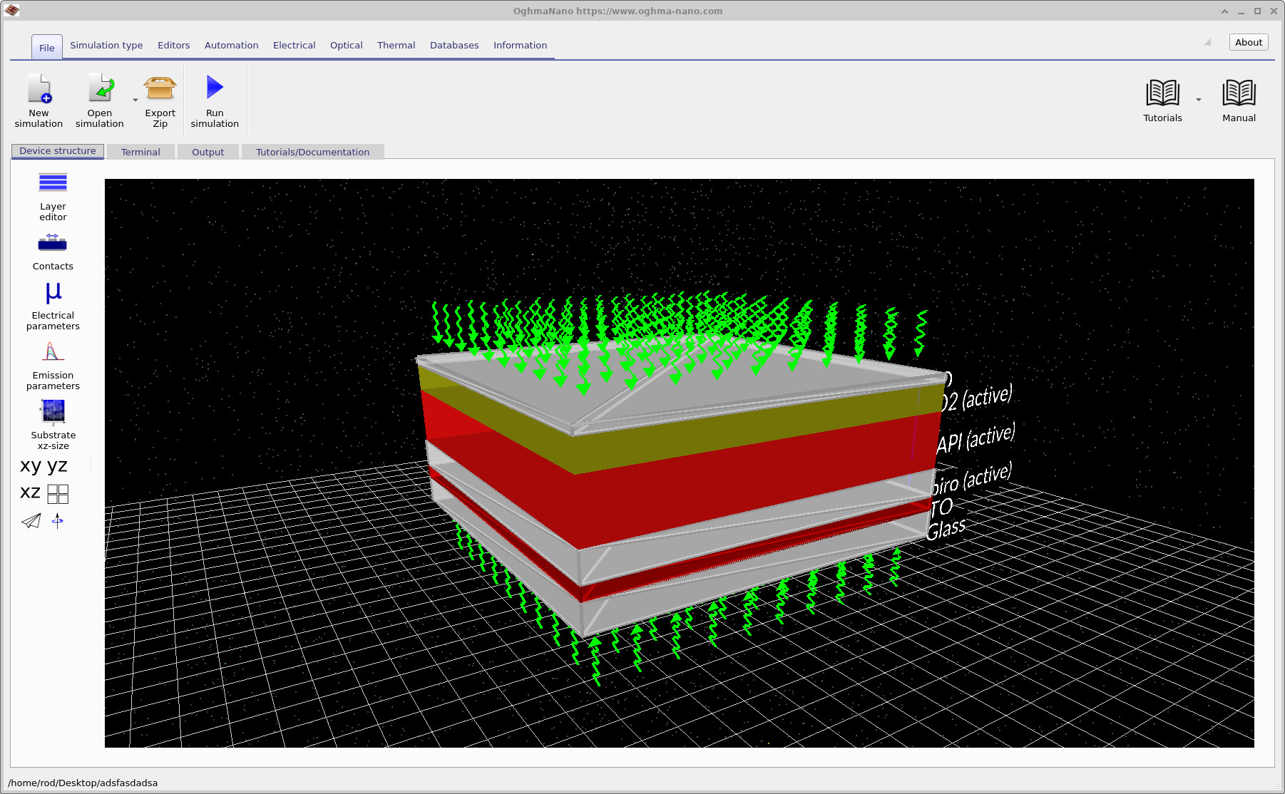
Once the simulation has loaded, the main OghmaNano window displays the bifacial device in the 3D visualisation panel, as shown in ??. Notice the green arrows indicating light entering the device from both the top and the bottom surfaces - this is the defining feature of bifacial operation. The layer stack visible in the 3D view is air / FTO / TiO₂ / MAPI / Spiro / ITO / Glass / air, where both the FTO and ITO contacts are transparent, enabling dual-sided illumination.
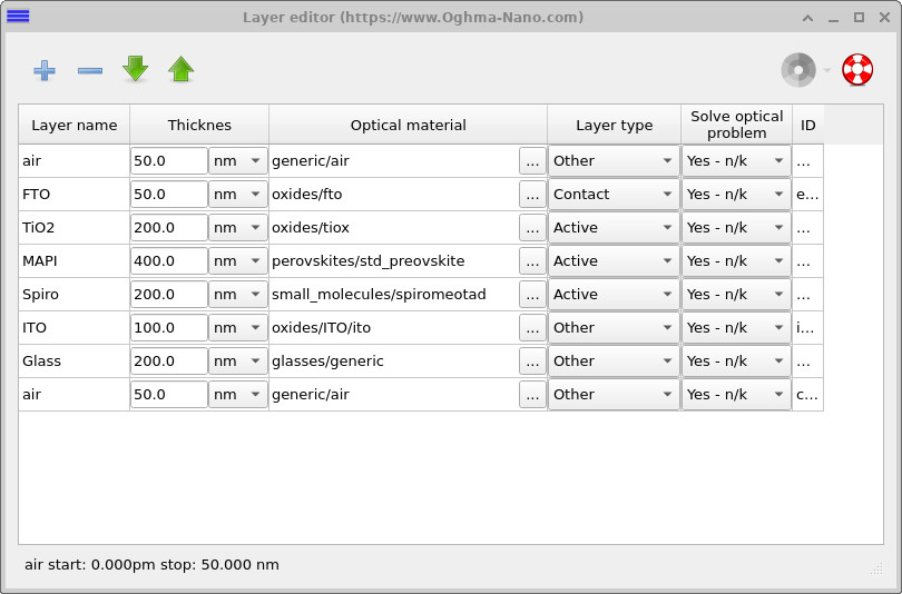
You can inspect the layer stack in detail by clicking Layer editor in the left-hand toolbar. The layer editor window, shown in ??, lists each layer with its thickness, optical material assignment, layer type (contact, active, or other), and whether the optical problem is solved for that layer. The bifacial stack includes ITO as the rear transparent contact and a Glass superstrate below, both of which allow rear-side light to enter the MAPI absorber.
3. Run the simulation and view the JV curve
Click the blue Run simulation button in the toolbar (or press F9) to
start the steady-state JV calculation. Once the simulation has finished, switch to the
Output tab. The output tab, shown in
??,
lists all result files written to the simulation directory.
Double-click jv.csv to open the JV curve viewer, as shown in
??.

jv.csv to plot the JV curve.

The most immediately striking feature of the bifacial JV curve is the short-circuit current density JSC. For a typical monofacial MAPbI₃ perovskite device under 1 Sun illumination, JSC is approximately 200–250 A m⁻². Here, with two 1 Sun light sources applied (one from each side), JSC is roughly doubled, reaching values approaching 500 A m⁻². This directly reflects the bifacial gain: both surfaces are harvesting photons and generating free carriers in the MAPI absorber. The open-circuit voltage VOC shows a more modest increase, because VOC depends logarithmically on photocurrent.
4. Inspect the light source configuration
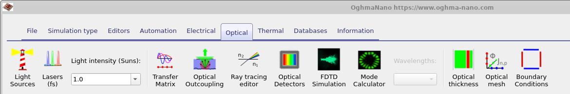
To understand how the dual illumination is configured, navigate to the Optical ribbon at the top of the main window (see ??) and click Light Sources. This opens the Light source editor, which lists all light source objects associated with the current simulation.
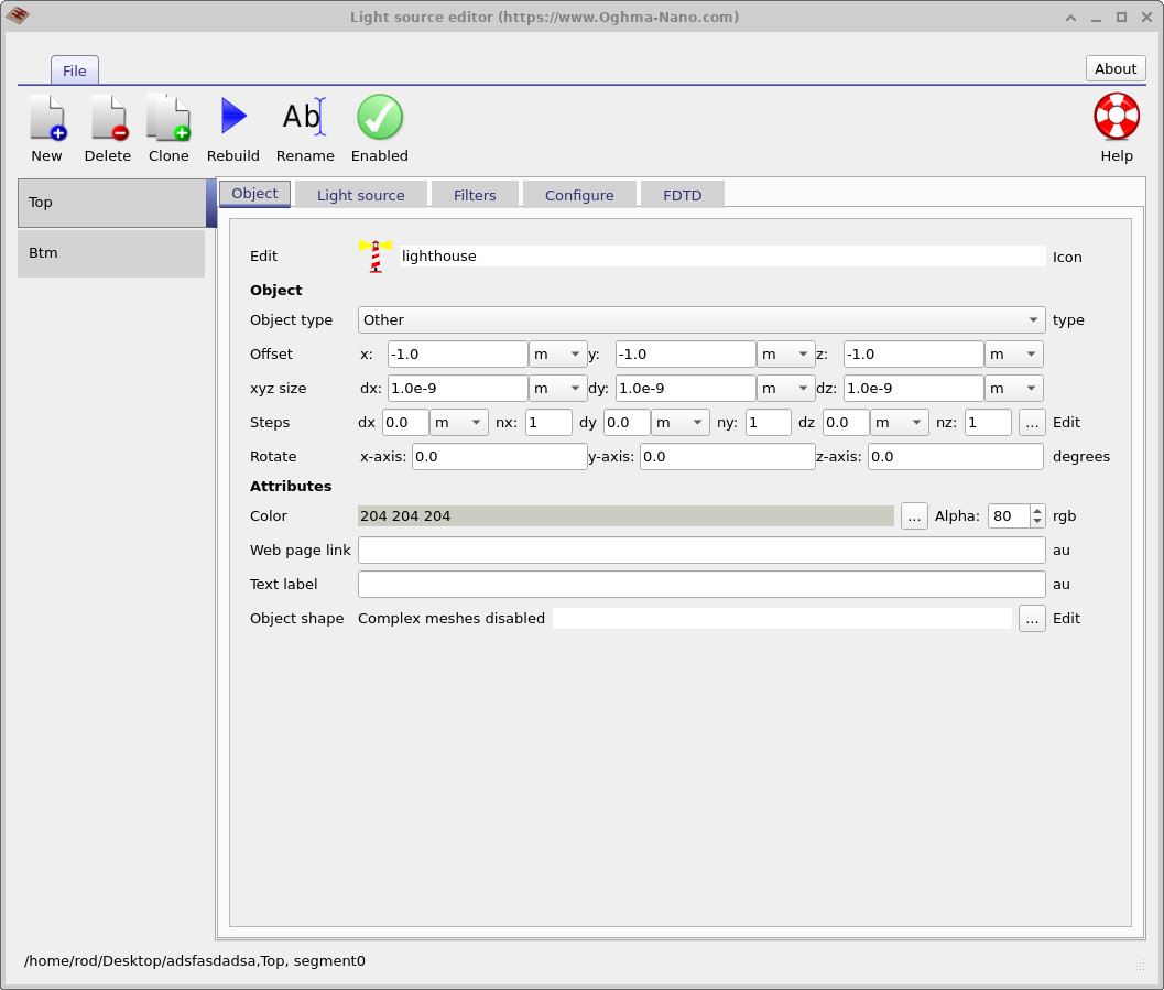
In the light source editor you will see two entries in the left panel: Top and Btm (bottom). Light sources are objects like any other object in OghmaNano — they have a physical x, y, z position and size, visible in the Object tab (??). For standard face illumination (top, bottom, left, right, front, back) these spatial properties are irrelevant — the light is assumed to arrive from outside the simulation window. They only become important if you place a light source at a specific position inside the device.
Click the Configure tab to set the Illuminate from direction. In this bifacial example, Top is set to Top (y0) (??) and Btm is set to Bottom (y1) (??).

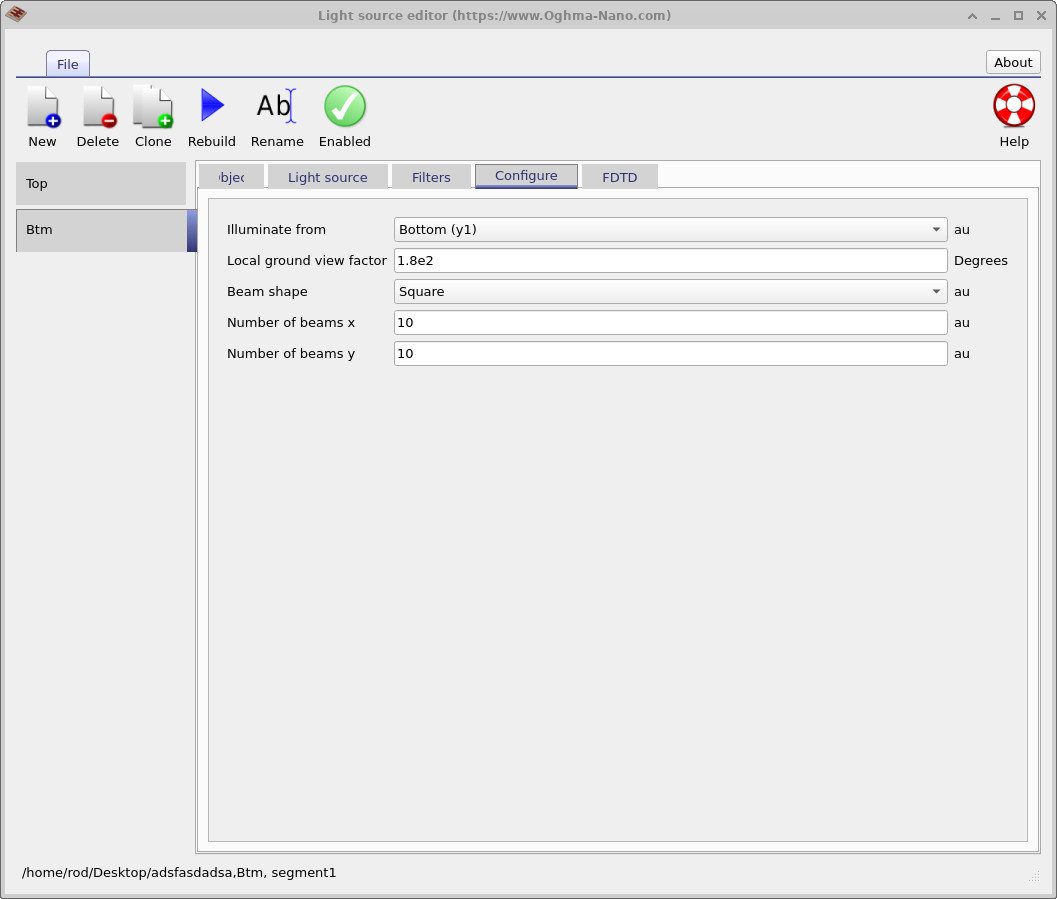
Together, these two light source objects replicate real-world bifacial operating conditions: direct solar irradiance enters from the top (y0) through the FTO contact, while diffuse or reflected irradiance enters from the bottom (y1) through the glass superstrate and ITO contact. Both sources use the same AM1.5G spectrum by default, which corresponds to the case where the rear irradiance equals the front irradiance - a useful upper bound for bifacial gain analysis. In practice, rear-side irradiance is typically 10–30% of front-side irradiance, which can be adjusted by modifying the light intensity in each source's Light source tab.
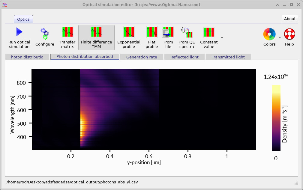
5. Optical analysis - photon distribution and absorbed photon density
After running the simulation, return to the Optical ribbon and click Transfer Matrix. This opens the optical simulation editor, which provides detailed visualisations of the optical field within the device. Three key outputs are shown in the figures below: the total photon distribution (??), the absorbed photon density (??), and the collapsed 1D generation rate profile (??).


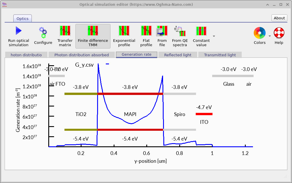
The generation rate profile in ?? shows a peak at each edge of the MAPI absorber — one at the TiO₂/MAPI interface (y ≈ 0.3 µm) where light enters from the top, and one at the MAPI/Spiro interface (y ≈ 0.7 µm) where light enters from the bottom. In a monofacial device only the first peak would be present, with the generation rate decaying exponentially through the absorber following Beer-Lambert absorption. The addition of rear-side illumination produces the second peak and raises the total integrated generation rate — and therefore JSC — by approximately a factor of two.
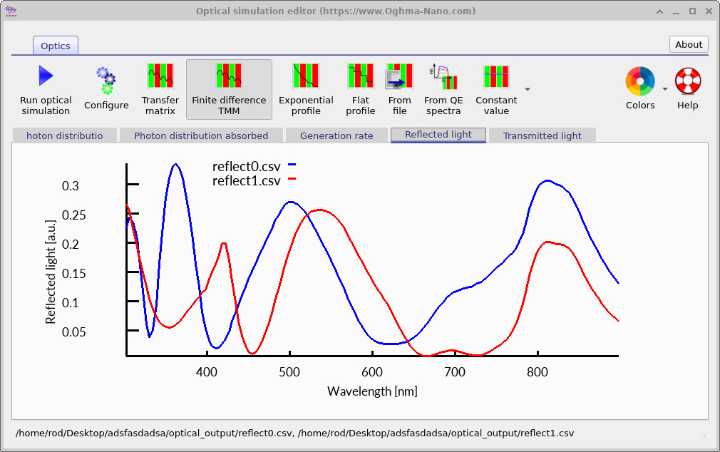
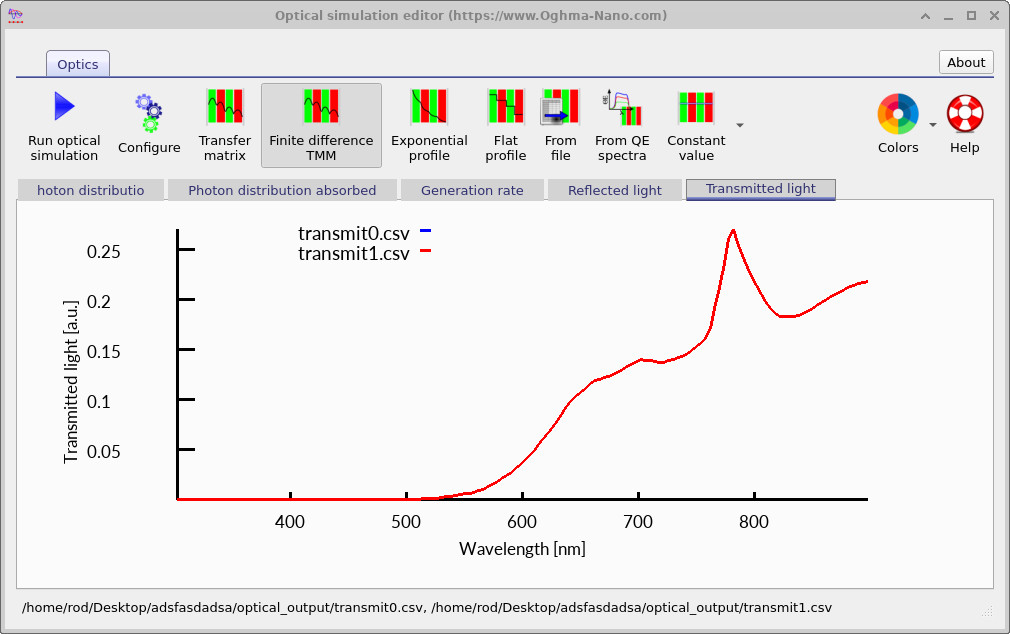
6. Reflectance and transmittance spectra
Still in the optical simulation editor, click the Reflected light tab (??) and then the Transmitted light tab (??). The reflection spectra from the top (reflect0.csv) and bottom (reflect1.csv) surfaces are clearly different — the oscillatory thin-film interference fringes are shifted in phase and amplitude because the sequence of interfaces encountered by incoming light is different from each side. The transmission spectra, however, are identical: transmit0.csv and transmit1.csv lie exactly on top of each other. This is a direct consequence of the optical reciprocity theorem, which states that the transmittance of a passive linear optical stack is the same regardless of which direction light travels through it. Reflectance has no such constraint — it depends on the specific interface sequence seen from each surface — which is why the two reflection spectra differ while the two transmission spectra do not.
💡 Show answer
Transmittance is governed by the optical reciprocity theorem: for any passive linear optical system (no gain, no nonlinear effects), the transmittance from port A to port B equals the transmittance from port B to port A. The total amount of light that passes completely through the stack is therefore the same regardless of illumination direction. Reflectance, by contrast, depends on the specific sequence of interfaces encountered by the incoming beam - which differs between the top and bottom surfaces - so reflect0.csv and reflect1.csv can, and generally do, differ.
7. Comparing single-sided illumination by disabling the bottom light source
To see how the optical distribution changes when only one light source is active, return to the Optical ribbon and click Light Sources to reopen the light source editor. In the left panel, select the Btm light source. In the toolbar at the top of the editor, the button currently reads Enabled (green tick icon). Click it to toggle the bottom light source to Disabled. Then click Run optical simulation in the optical simulation editor to update the optical output with only the top light source active.
The updated photon distribution, absorbed photon density, and 1D generation rate profile under single-sided (top-only) illumination are shown below in ??, ??, and ??.

The contrast between the bifacial and monofacial optical results clearly illustrates the physical origin of the bifacial current enhancement. With only the top light source active, the generation rate peaks sharply near the illuminated interface and decays exponentially through the absorber. With both sources active, a second, symmetric peak appears from the rear, and the total integrated generation rate - and therefore JSC - is approximately doubled.
Summary and what you have learned
This tutorial has introduced bifacial perovskite solar cell simulation in OghmaNano using a MAPbI₃ device with an air / FTO / TiO₂ / MAPI / Spiro / ITO / Glass / air stack. You have seen that replacing the opaque rear contact with a transparent ITO layer allows light to enter from both surfaces simultaneously, approximately doubling JSC while VOC increases only modestly due to its logarithmic dependence on photocurrent. The generation rate profile — peaking at both edges of the MAPI absorber — is the direct optical signature of this dual illumination. Inspection of the reflectance and transmittance spectra confirmed that while the two reflection spectra differ (the interface sequence seen from each surface is different), the transmission spectra are identical in both directions, as required by the optical reciprocity theorem. Finally, disabling the bottom light source showed how the generation profile collapses to a single peak and absorption becomes asymmetric, recovering the familiar monofacial behaviour.
👉 Next steps:
- Try modifying the intensity of the bottom light source (in its Light source tab) to values of 0.1 and 0.3 Suns, which correspond to more realistic rear irradiance levels in a bifacial field installation. Observe how JSC, VOC, and PCE change.
- Return to the Perovskite Tutorial Part B to explore how the optical stack and absorber thickness affect the optical performance of a monofacial device.
- Explore the perovskite solar cell simulation overview for a broader introduction to the physics implemented in OghmaNano.