Anti-Reflective Coating Simulation (Transfer Matrix Method): Quarter-Wave Thin-Film Tutorial
In this tutorial you will simulate a single-layer anti-reflective coating using the transfer matrix method (TMM). You will build a quarter-wave thin-film optical coating, calculate reflection and transmission spectra, examine the photon density distribution inside the structure, and investigate how coating thickness changes the wavelength of minimum reflection.
1. Introduction
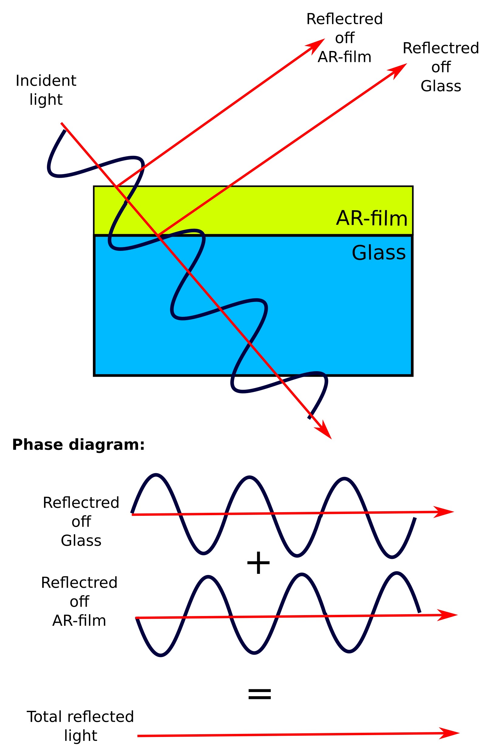

At an interface between two materials with different refractive indices, an incident optical wave generally splits into reflected and transmitted components. As a result, even transparent optical surfaces such as glass or dielectric coatings reflect a fraction of the incoming light. In many optical systems this reflection represents a loss mechanism because it reduces optical coupling and limits the amount of light reaching the active region of the device.
Anti-reflective coatings reduce this reflection using thin-film interference. As illustrated in ??, a thin dielectric film is inserted between air and the substrate. Reflection now occurs at both the air-film and film-substrate interfaces. If the optical thickness of the film is chosen correctly, the two reflected waves acquire a phase difference of approximately \(\pi\), causing destructive interference and suppressing the net reflected field.
For normal incidence, the destructive interference condition is approximately
\(d = \dfrac{\lambda_0}{4n_f}\)
where \(d\) is the coating thickness, \(n_f\) is the refractive index of the film, and \(\lambda_0\) is the target free-space wavelength. This is the well-known quarter-wave coating condition. In practice, anti-reflective coatings are widely used in solar cells, photodetectors, imaging systems, dielectric mirrors, and precision optical instrumentation.
In this tutorial we model a single-layer anti-reflective coating using the transfer matrix method (TMM). TMM solves the optical problem by matching forward and backward travelling electromagnetic waves across planar interfaces, making it extremely efficient for layered one-dimensional structures. Unlike full-wave spatial solvers, the transfer matrix method directly computes reflection, transmission, and optical field distributions without explicitly propagating the fields through time.
The structure used in this tutorial is shown conceptually in ??. We will calculate reflection and transmission spectra, visualise the standing-wave photon density inside the structure, and investigate how the coating thickness shifts the wavelength of minimum reflection.
For a comparison with a full electromagnetic time-domain simulation of the same structure, see the companion tutorial: Anti-reflective coating simulation using FDTD.
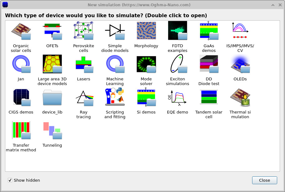
2. Making a new simulation
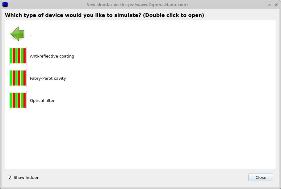
Open the New simulation window and select the Transfer matrix method category (??). Then select the Anti-reflective coating example (??). This loads the main interface shown in ??.
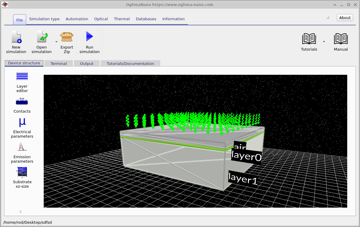
The structure consists of air, a thin anti-reflective coating layer, and a thick gallium arsenide (GaAs) substrate. The coating layer has a refractive index near \(n=2\), while the substrate uses the measured optical constants for GaAs.
Although this is a very simple layered structure, it already demonstrates many of the key physical ideas behind thin-film optics: interference, phase matching, standing-wave formation, wavelength-selective reflection suppression, and resonant optical enhancement.
3. Examining the layer structure

Open the Layer editor from the left-hand toolbar. The layer structure is shown in ??.
The structure contains three regions:
- Air - the incident medium.
- The anti-reflective coating - a thin \(n=2\) dielectric layer.
- The GaAs substrate - the absorbing semiconductor.
The coating thickness is initially set to approximately 44 nm. This corresponds roughly to a quarter-wave thickness for blue light around 350-400 nm. At this wavelength the reflected waves from the two interfaces become out of phase and cancel.
The transfer matrix method treats each layer as a homogeneous optical slab. Maxwell's equations are solved analytically within each layer, and the fields are connected across interfaces using boundary conditions. The resulting matrix formalism allows the total reflection and transmission to be calculated extremely efficiently.
4. Running the optical simulation
Open the Optical tab, shown in ??. This contains the transfer matrix controls and optical analysis tools.
Click the Transfer Matrix button to open the optical simulation editor. Then press the Run optical simulation button.
The simulation calculates:
- The photon density inside the structure.
- The reflected optical power.
- The transmitted optical power.
- The absorbed photon distribution.
Because the transfer matrix method solves the layered structure analytically, the simulation typically completes almost instantly. This makes TMM ideal for rapidly exploring coating thicknesses and optical designs.
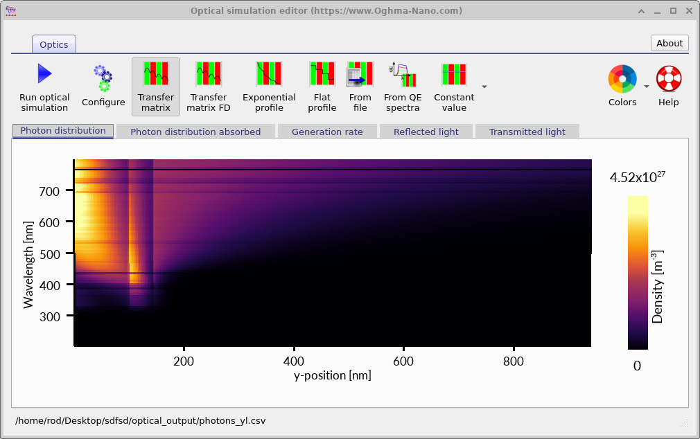
5. Photon density distribution
The photon density distribution is shown in ??. The horizontal axis corresponds to position inside the structure, while the vertical axis corresponds to wavelength.
Several important physical effects can be observed:
- At shorter wavelengths the GaAs substrate absorbs strongly, so the photon density decays rapidly after entering the material.
- Near the anti-reflective design wavelength, the standing-wave pattern near the interface is reduced, indicating reduced reflection.
- At longer wavelengths the absorption coefficient decreases, allowing light to penetrate deeper into the substrate.
The bright interference features near the coating layer arise from coherent interference between forward- and backward-propagating waves. These standing-wave effects are naturally captured by the transfer matrix method.
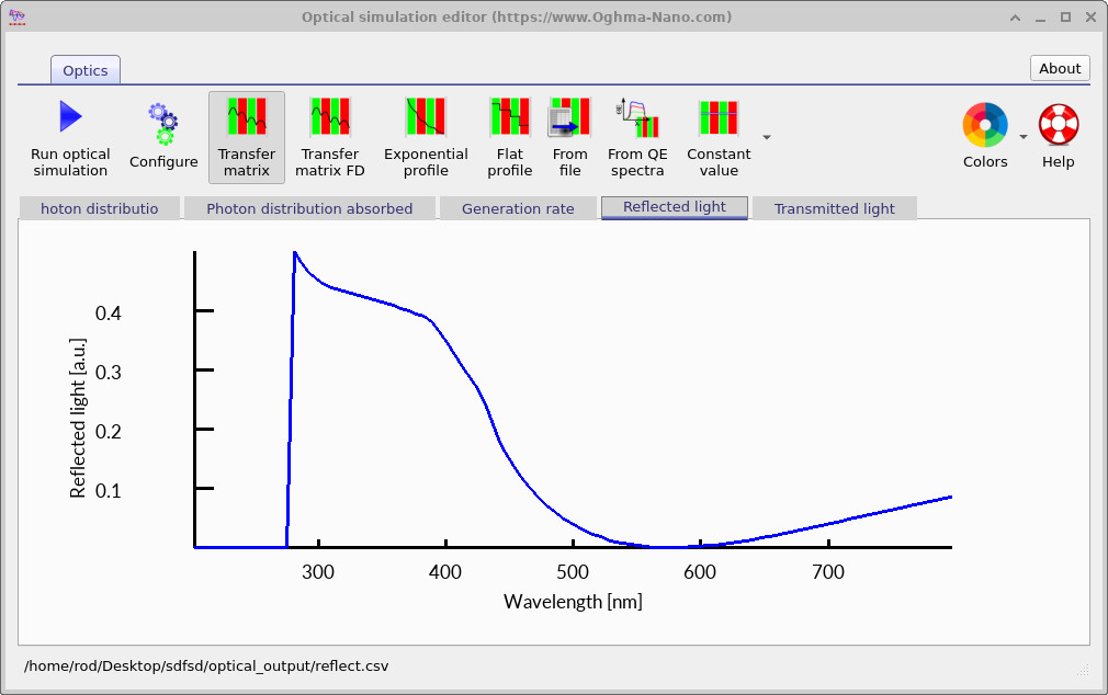
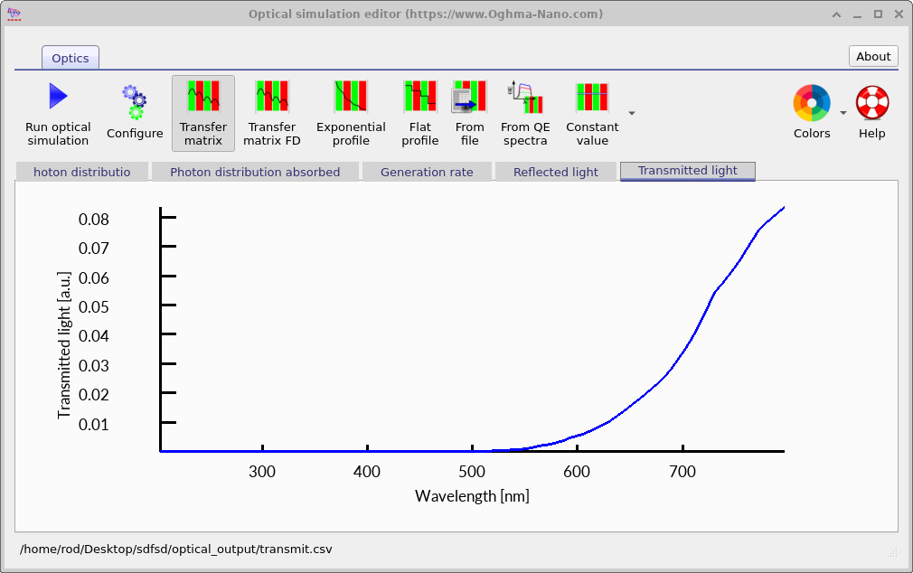
6. Reflection and transmission spectra
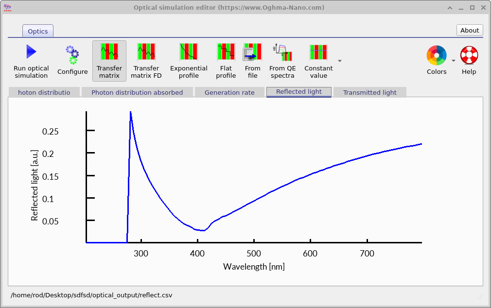
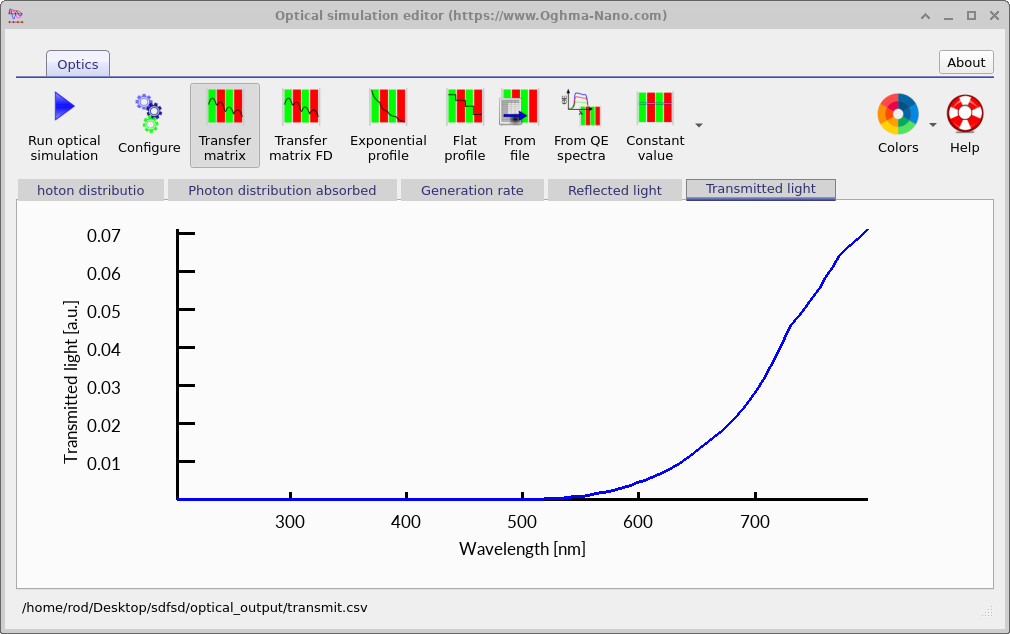
The reflected and transmitted spectra are shown in ?? and ??.
The reflection spectrum shows a pronounced minimum near 400 nm. This is the wavelength for which the quarter-wave interference condition is approximately satisfied. At this wavelength, the reflected waves from the two interfaces interfere destructively, reducing the net reflected power.
Correspondingly, the transmission spectrum increases near the same wavelength, because less light is lost to reflection.
Away from the design wavelength, the phase condition is no longer satisfied, so the reflected intensity rises again. This is why single-layer anti-reflective coatings are generally narrow-band devices.
7. Examining the outputs
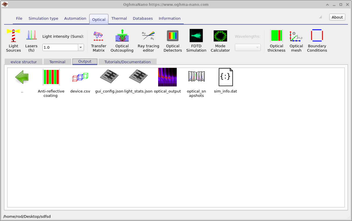
After the simulation completes, the generated files are listed in the Output tab, shown in ??.
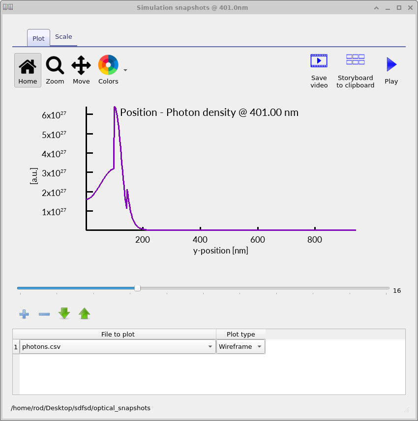
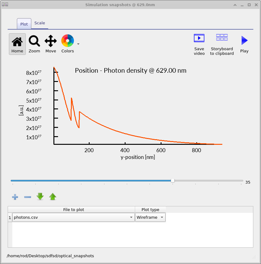
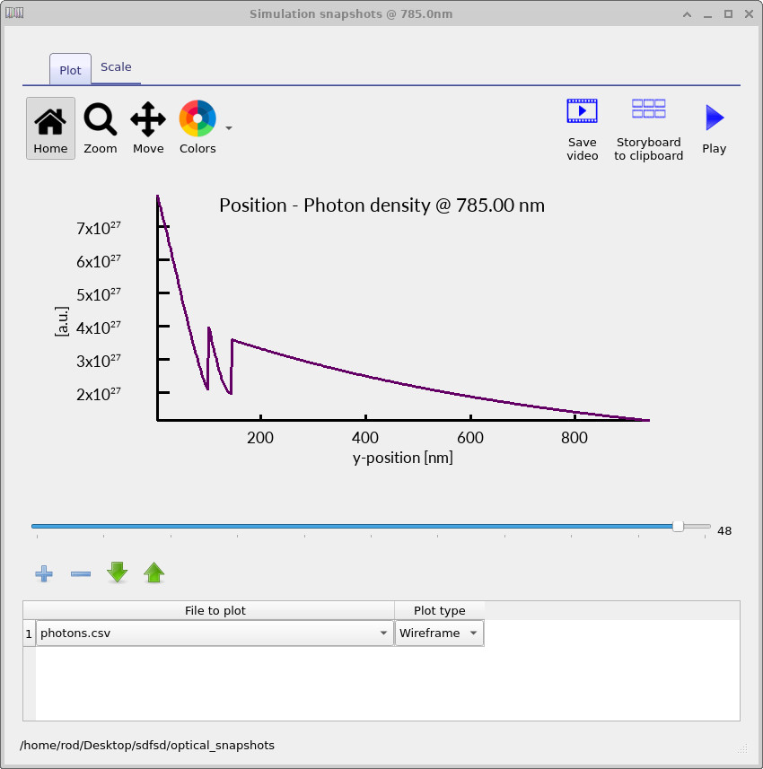
Open the optical_snapshots/ directory and launch the snapshot viewer.
Example wavelength snapshots are shown in
??-
??.
These snapshots show the photon density distribution inside the structure at individual wavelengths.
At wavelengths close to the anti-reflective condition, the standing-wave intensity near the surface is reduced, indicating reduced reflection and improved optical coupling into the substrate.
At longer wavelengths, the substrate absorption decreases, allowing the optical field to penetrate more deeply into the material.
9. Try it yourself: changing the coating thickness
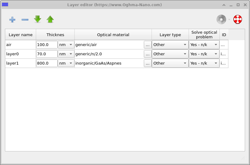
Return to the Layer editor and increase the coating thickness from 44 nm to 70 nm, as shown in ??.
Rerun the optical simulation and compare the new spectra, shown in ?? and ??.
You should observe that the reflection dip moves from roughly 400 nm toward 550-600 nm. Correspondingly, the transmission enhancement also shifts to longer wavelengths.
10. Comparing TMM and FDTD
This tutorial used the transfer matrix method to analyse a layered optical coating. TMM is particularly powerful for planar multilayer systems because it is:
- Extremely fast.
- Numerically stable.
- Well suited to layered structures.
- Easy to use for thickness optimisation.
However, the transfer matrix method assumes laterally uniform layers. If the structure becomes strongly non-planar, or if full wave propagation in two or three dimensions is required, methods such as FDTD become more appropriate.
For comparison, see the companion tutorial: Anti-reflective coating simulation using FDTD.
Using both methods together is often extremely useful: TMM provides a rapid reference solution for ideal layered systems, while FDTD provides more direct physical insight into field propagation and non-planar effects.