OghmaNano provides a dedicated workflow for designing and analysing multilayer optical filters, reflective coatings, anti-reflection stacks, and other thin-film optical structures. Using its optical filter tutorial and built-in optical solvers, you can calculate wavelength-dependent reflection, transmission, absorption, and photon distribution through arbitrary layer stacks.
This makes OghmaNano useful not only for stand-alone filter design, but also for broader optoelectronic problems where thin-film optics matters — for example solar cells, OLED stacks, perovskite devices, and other layered photonic structures. In these systems, the optical coating is often not a separate problem: it is part of the device itself.
The software is therefore useful both as a fast design environment for coatings and filters, and as a hub for exploring how thin-film optics couples into full device simulations. If you want to move from a simple multilayer mirror to a full optoelectronic stack, the same optical concepts carry over naturally.
At the core of this workflow is a transfer-matrix optical model, which is ideal for layered thin-film structures at normal incidence. This allows you to calculate the spectral response of multilayer filters quickly and with high accuracy. A single quarter-wave layer can be used as an anti-reflection coating, while alternating high- and low-index layers form Bragg reflectors, band-stop filters, and narrowband mirrors. The same formalism is described in the optical filter tutorial, where the stack is built and the resulting spectra are interpreted.
Because OghmaNano stores optical constants in a large materials database, you can move directly from generic textbook designs to stacks based on real materials. Changing layer thickness or refractive index immediately shifts the passband and stopband structure, making the software useful both for initial concept work and for matching a design to a real experiment.
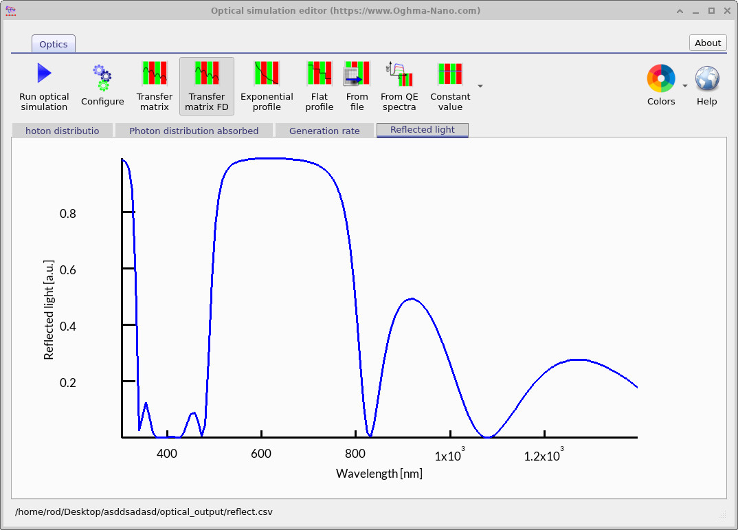
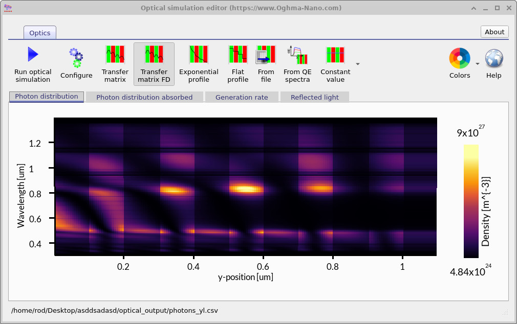
The same approach is also useful for reflective coatings on photonic structures, wavelength-selective mirrors, and practical anti-reflection coatings for optoelectronic devices. Rather than only giving a final reflectance curve, OghmaNano also lets you inspect the internal photon distribution and where absorption is taking place, which is often the difference between a design that looks right on paper and one that actually works.
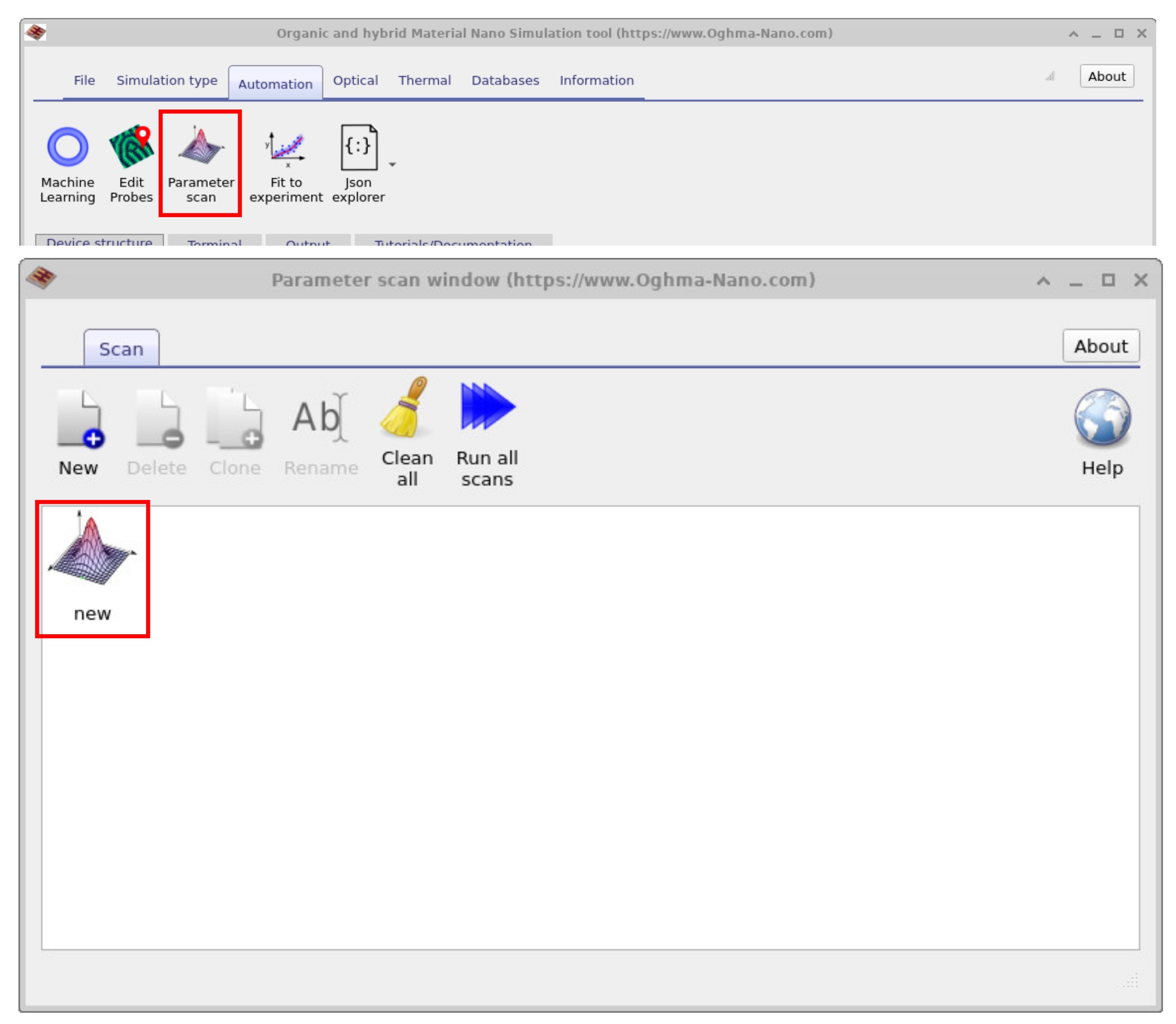
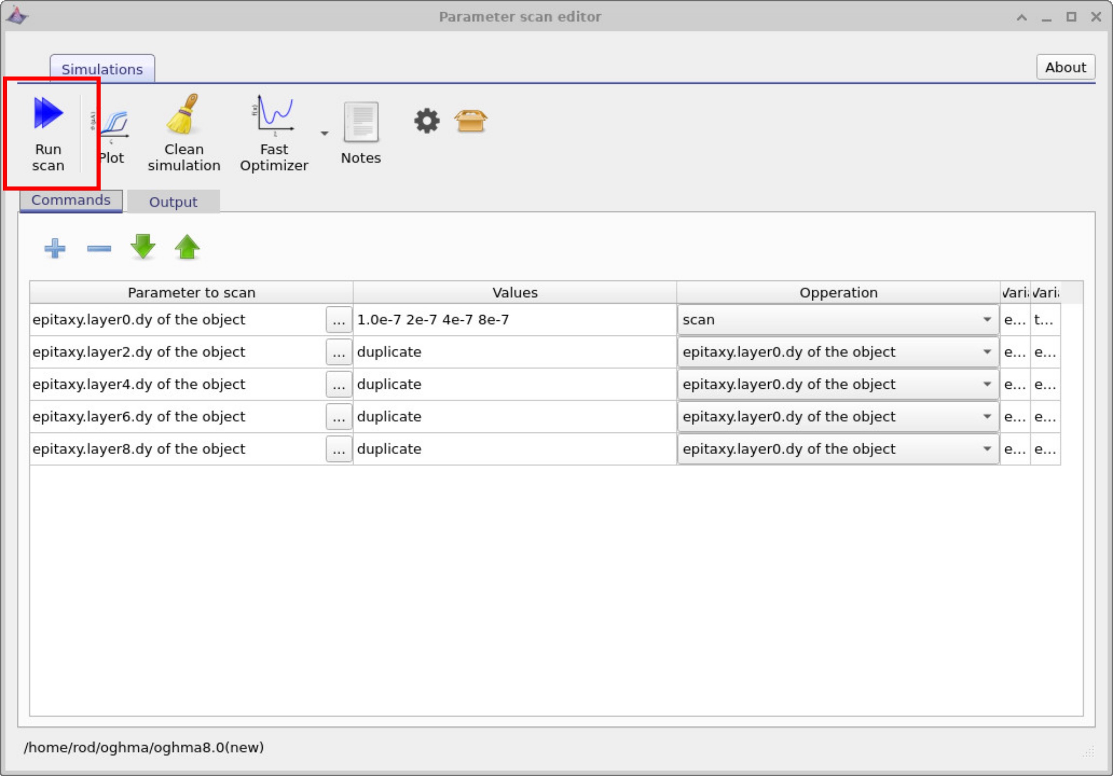
If you want to move beyond a single design and explore the parameter space systematically, OghmaNano also includes automated parameter scanning for optical filters. This makes it easy to scan layer thicknesses, duplicate changes across repeated layers, and compare many candidate filters side by side.
One of the strengths of OghmaNano is that optical filter design does not sit in isolation. The same optical stack formalism used for coatings and filters also appears inside broader transfer-matrix optical simulations for optoelectronic devices. In practice, this means the same skills used to design a dielectric mirror or antireflection coating can be transferred directly into modelling the front stack of a solar cell, an OLED outcoupling structure, or a layered photodetector.
If your problem goes beyond ideal planar thin films, OghmaNano also includes broader optical tools such as ray tracing and wave-optical modelling workflows elsewhere in the software. The filter-design page is therefore a good entry point into the wider optical side of OghmaNano.
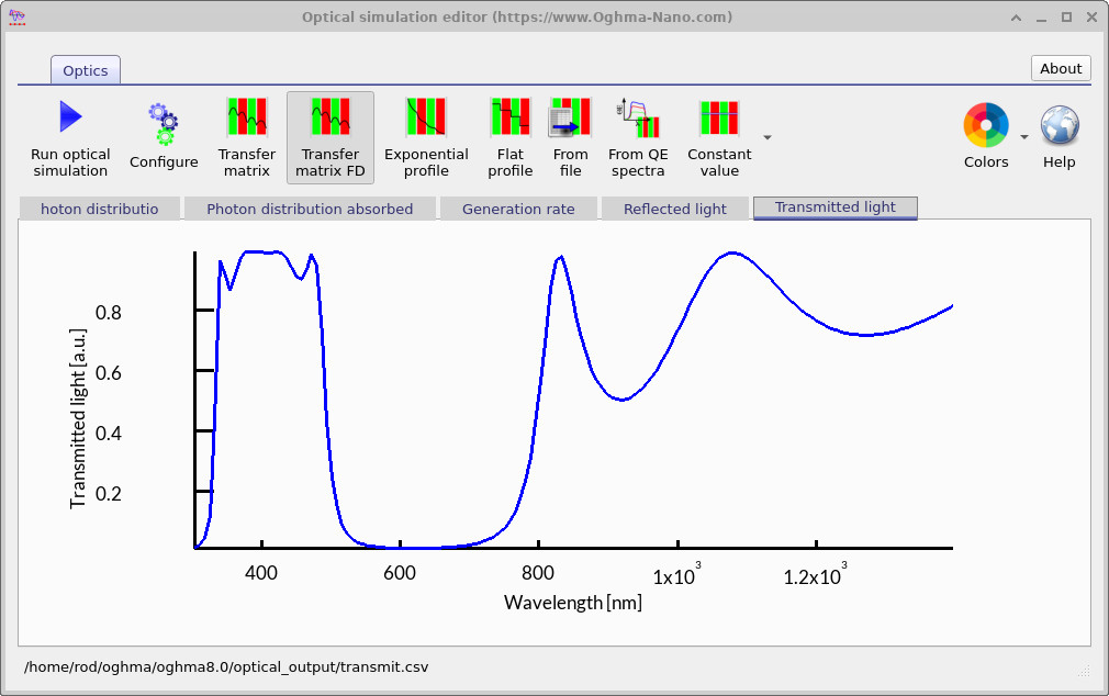
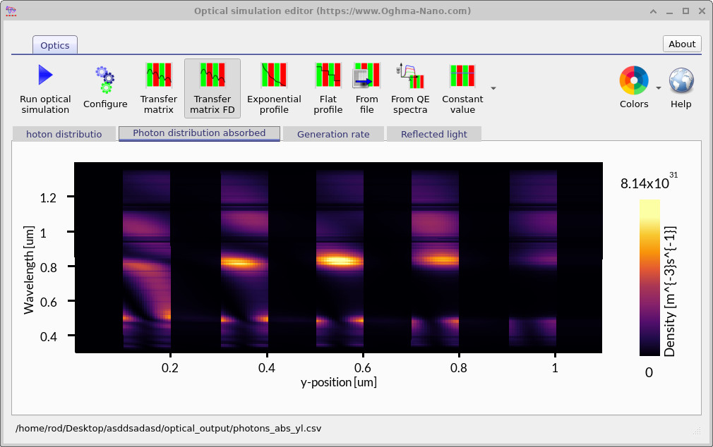
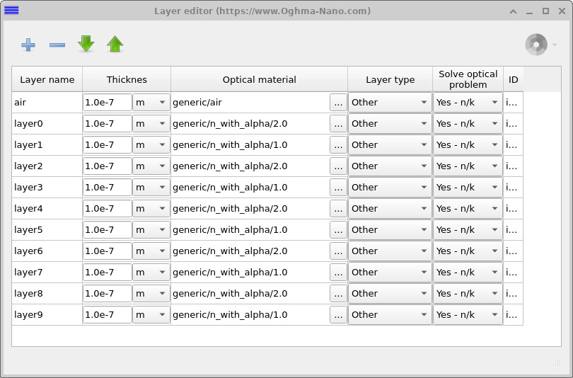
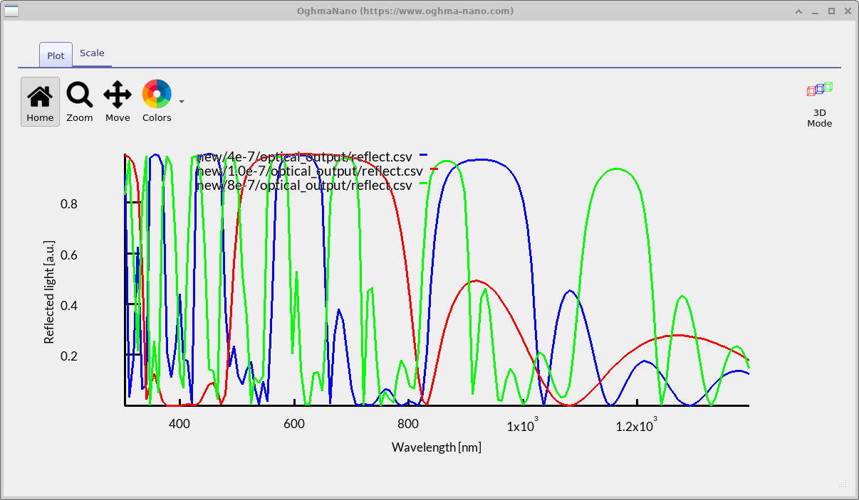
A particularly useful part of the filter workflow is the ability to scan thickness systematically. In Part B of the optical filter tutorial, one layer thickness is scanned across several values and then duplicated across the repeated high-index layers in the stack. This produces a family of filters which can then be compared using combined reflectance and transmittance plots.
That is a powerful design pattern: rather than guessing a single stack, you can evaluate many related designs automatically and identify where the stopband moves, where transmission reappears, and how absorption changes. For practical filter design, this is often more useful than manually editing one layer at a time.
If you are new to this part of the software, start with the optical filter tutorial, then continue to Part B on automated thickness scans. If your interest is broader thin-film optics in device structures, the transfer-matrix side of OghmaNano also connects naturally to transfer-matrix optical theory and to device-level examples such as solar cells, perovskite devices, and OLED simulation.
Want to dive deeper?
👉 Start with Part A: Optical filter basics, then continue to Part B: automating and scanning thickness.