What are organic semiconductors? Materials, devices and applications
1. What are organic semiconductors?
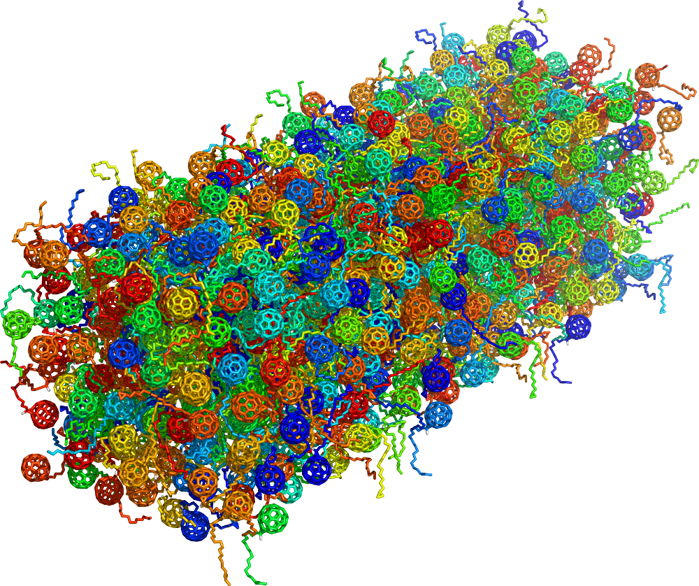
Organic semiconductors are carbon-based electronic materials made from conjugated polymers and small molecules. They are used to build organic electronic devices such as organic solar cells, OLEDs and organic field-effect transistors. Unlike crystalline inorganic semiconductors such as silicon or III-V compounds, organic semiconductors are usually structurally and energetically disordered molecular systems rather than periodic solids (see ??).
This means organic semiconductors should not be treated as low-performance versions of silicon. They are a different class of semiconductor. Their electronic behaviour is controlled by localized molecular states, energetic disorder, trap occupation, exciton formation and nanoscale morphology. These features make organic electronics technologically attractive, but they also make organic semiconductor device modelling physically distinct from conventional crystalline semiconductor simulation.
2. How organic semiconductors differ from inorganic semiconductors
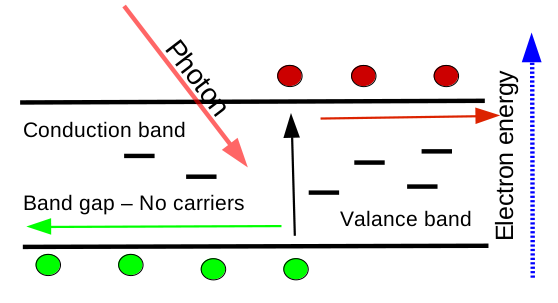
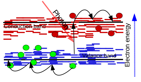
In crystalline semiconductors, atoms are arranged in a periodic lattice and carriers can often be described using extended band states. This gives rise to relatively well-defined conduction and valence bands, as shown in ??. In organic semiconductors, the molecular packing is less ordered and the local electronic environment varies from site to site. The result is a broad density of localized states rather than a sharp band edge (??).
Charge transport in organic materials is therefore often described as thermally activated hopping between localized states rather than band-like transport through extended states. Carriers can become trapped in low-energy states, released later by thermal activation, and recaptured elsewhere. This makes the apparent mobility strongly dependent on temperature, carrier density, electric field, energetic disorder and trap occupation.
Another major difference is exciton physics. In many organic optoelectronic materials, optical absorption produces bound electron-hole pairs called excitons rather than immediately generating free carriers. Whether an absorbed photon produces useful electrical current depends on exciton diffusion, dissociation, recombination and the nanoscale arrangement of donor and acceptor materials.
3. Organic semiconductor materials: polymers and small molecules
Organic semiconductor materials are usually divided into two broad classes: conjugated polymers and small molecules. Polymers consist of long molecular chains with delocalized \(\pi\)-electron systems along the backbone, while small molecules are lower molecular-weight compounds designed to have suitable frontier orbital energies, absorption spectra and packing behaviour.
The advantage of this chemical flexibility is that the optical gap, energy levels, solubility, crystallinity and morphology can be tuned through molecular design. This is one reason organic materials are attractive for photovoltaics, light emission, sensors and flexible electronics. The disadvantage is that device behaviour can be extremely sensitive to processing conditions, phase separation, molecular orientation and interfacial structure.
4. Organic electronic devices
Organic semiconductors are used in several major classes of organic electronic and optoelectronic devices. In each case, the device behaviour is determined not only by the electronic properties of the material, but also by optical absorption, morphology, interfaces, contacts and recombination.
- Organic photovoltaics (OPVs) convert absorbed light into electrical current. They usually rely on donor-acceptor heterojunctions to split excitons into free carriers. See the organic solar cell simulation tutorial for a practical OghmaNano example.
- Organic light-emitting diodes (OLEDs) inject electrons and holes into organic layers, where they recombine to form emissive excited states. Optical interference, recombination-zone position and outcoupling can strongly affect the final emission. See the OLED coherent thin-film optics tutorial.
- Organic field-effect transistors (OFETs) use a gate field to accumulate charge at an organic semiconductor interface. Their output is controlled by contact injection, mobility, interfacial disorder and trap-limited transport. See the OFET simulation tutorial.
5. Why modelling organic semiconductors is different
Organic semiconductor simulation must treat disorder and trap states explicitly. A simple drift-diffusion model with constant mobility and band-to-band recombination is often insufficient because carrier density, mobility, recombination and internal electric field are coupled through the density of states and trap occupation.
For example, changing the illumination intensity or applied voltage changes the trap filling. Trap filling changes the free-carrier density. The free-carrier density changes recombination and conductivity. The resulting change in charge distribution then modifies the internal electric field and extraction. This feedback loop is one reason why organic device models must include trap-state physics.
Recombination is often trap-assisted and is commonly described using Shockley–Read–Hall recombination. In disordered organic semiconductors, SRH-type models are not just a minor correction: they are often essential for describing carrier capture, emission and recombination through localized states. This is why organic device simulation is best understood as coupled transport, trapping, recombination and electrostatics rather than as a simple current-flow calculation.
6. Advantages of organic semiconductors
Organic semiconductors are attractive because they can be processed in ways that are difficult or expensive for conventional inorganic semiconductors. Many organic materials can be deposited at low temperature, processed from solution, printed over large areas and integrated onto lightweight or flexible substrates.
These properties make them interesting for applications where mechanical flexibility, low-temperature fabrication, large-area coating or spectral tunability matter more than achieving the highest possible carrier mobility. OLED displays are the clearest commercial example, but organic semiconductors also remain important for photovoltaics, photodetectors, sensors, wearable devices and low-cost electronics.
7. Limitations and challenges
The same disorder that enables flexible processing also creates limitations. Organic semiconductors usually have lower mobility than crystalline inorganic materials, stronger trap effects and greater sensitivity to morphology. Stability can also be a major issue, especially under oxygen, moisture, heat, high current density or prolonged illumination.
Interfaces are especially important. Contact selectivity, injection barriers, interfacial traps and morphology near electrodes can dominate device behaviour. This is why the measured performance of an organic device is often not a property of the active material alone, but of the complete device stack, processing history and measurement conditions.
8. Where organic semiconductors may win
Organic semiconductors are unlikely to replace crystalline silicon in every application. Silicon remains dominant where high mobility, long-term stability and mature high-volume manufacturing are decisive. Organic materials are more likely to win where their distinctive properties matter: mechanical flexibility, low-temperature processing, lightweight devices, tunable absorption or emission, and compatibility with large-area manufacturing.
OLED displays show that organic semiconductors can dominate when the device physics, materials engineering and manufacturing route are well matched. Future opportunities include flexible photovoltaics, indoor energy harvesting, organic photodetectors, biomedical sensors, wearable electronics and hybrid systems where organic materials are integrated with inorganic or perovskite technologies.
9. Simulating organic semiconductors in OghmaNano
OghmaNano is designed to simulate organic semiconductor devices as coupled optical, electrical and morphological systems. It includes drift-diffusion transport, trap-state distributions, SRH and non-equilibrium recombination, exciton dynamics, optical generation and frequency-domain characterisation in a single workflow.
For a practical overview of the available tutorials, see organic semiconductor device simulation. That page links to OPV, OLED, OFET, SCLC, exciton, bulk-heterojunction and frequency-domain examples.