OLED Optical Outcoupling Simulation Using the Transfer Matrix Method (TMM)
1. Introduction
In this tutorial you will simulate optical outcoupling in an organic light-emitting diode (OLED) using the transfer matrix method (TMM).
Unlike solar-cell simulations where light enters the device and is absorbed, OLED optical simulations begin with photons generated inside the emissive layer. The transfer matrix solver then calculates how these photons propagate through the multilayer stack and determines the probability that they escape from the device into free space.
OLEDs are strongly influenced by optical interference because the device thickness is comparable to the optical wavelength. Light emitted inside the device reflects repeatedly from the metallic electrode and dielectric interfaces, producing standing-wave patterns and optical cavity effects.
These cavity effects strongly influence the final emission spectrum, angular emission profile, colour purity, and optical outcoupling efficiency of the OLED.
In practical devices, only a fraction of the internally generated photons escape into free space. Many photons become trapped in guided modes, substrate modes, or surface-plasmon modes at the metal interface. Understanding and optimising optical outcoupling is therefore one of the key challenges in OLED design.
2. Creating the OLED simulation
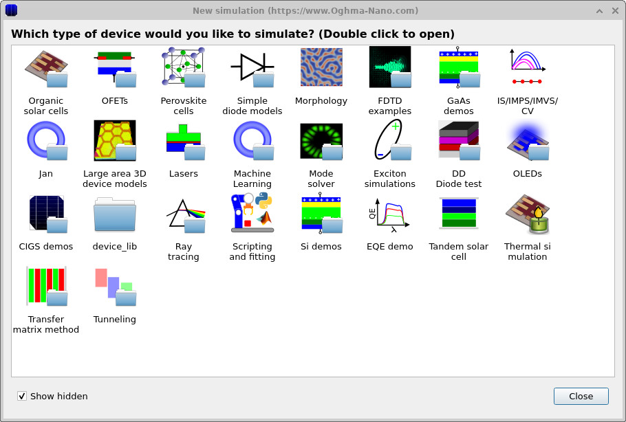
Open the New simulation window shown in ??. Select the OLEDs category.
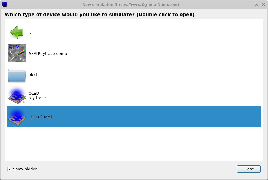
Inside the OLED category select the OLED (TMM) example shown in ??.
Save the simulation to a suitable directory on disk. Once loaded, the main simulation interface shown in ?? will appear.
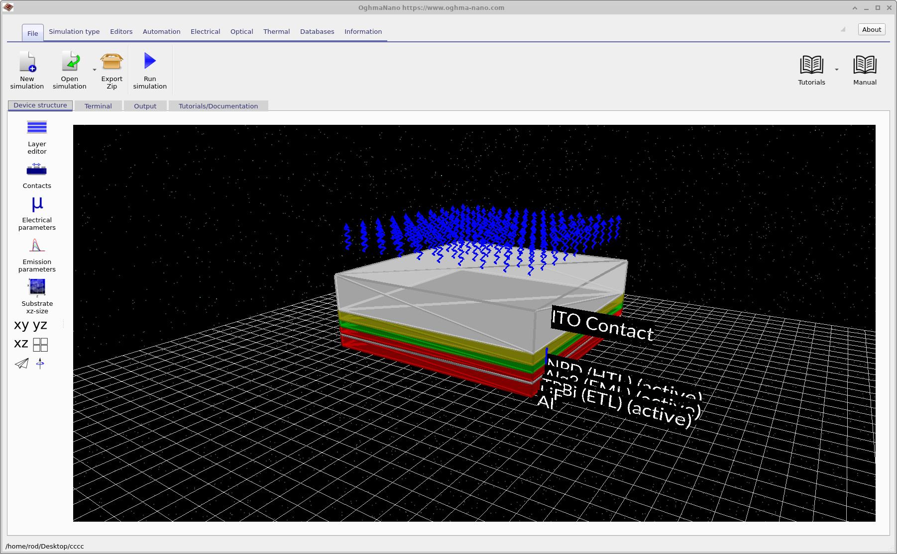
The example contains a complete multilayer OLED structure including a transparent ITO contact, hole transport layer, emissive layer, electron transport layer, and metallic cathode.
3. Examining the OLED structure
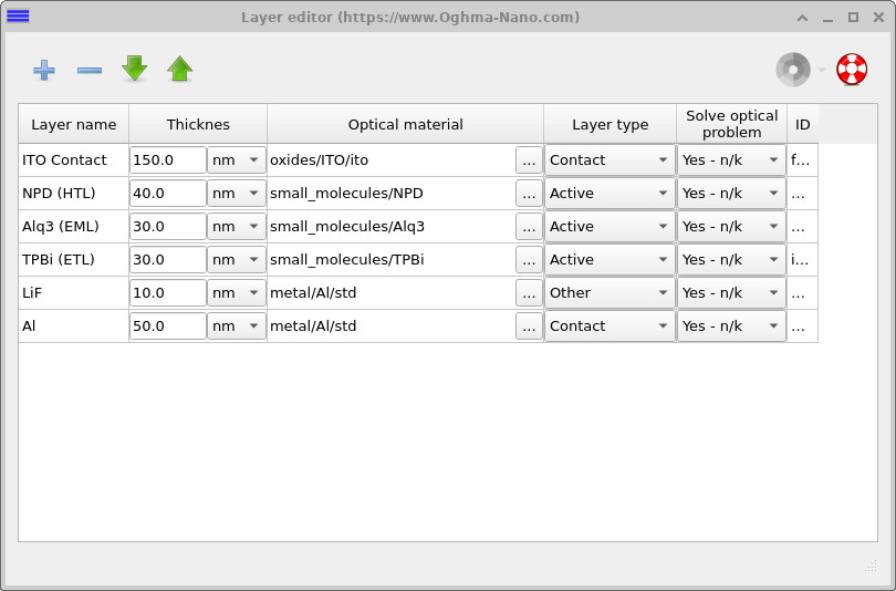
Open the Layer editor from the left-hand toolbar. The multilayer OLED stack shown in ?? will appear.
The device consists of an ITO transparent anode, an NPD hole transport layer (HTL), an Alq3 emissive layer (EML), a TPBi electron transport layer (ETL), a LiF interfacial layer, and an aluminium cathode.
The aluminium cathode acts as a highly reflective mirror, producing a resonant optical cavity inside the OLED. Light emitted from the emissive layer reflects repeatedly inside this cavity, strongly modifying the optical field distribution and escape probability.
Because the optical cavity modifies the local density of optical states, the thickness of each OLED layer can substantially alter the emission efficiency and spectrum.
4. Opening the optical outcoupling solver
Open the Optical tab shown in ??.
Click the Optical Outcoupling button to open the OLED outcoupling simulation window.
Unlike solar-cell optical simulations, OLED outcoupling simulations calculate the propagation of internally generated photons rather than externally incident light.
The transfer matrix solver calculates the optical electric field distribution, cavity resonances, photon escape probability, and wavelength-dependent outcoupling efficiency throughout the multilayer OLED stack.
5. Configuring the emission layer
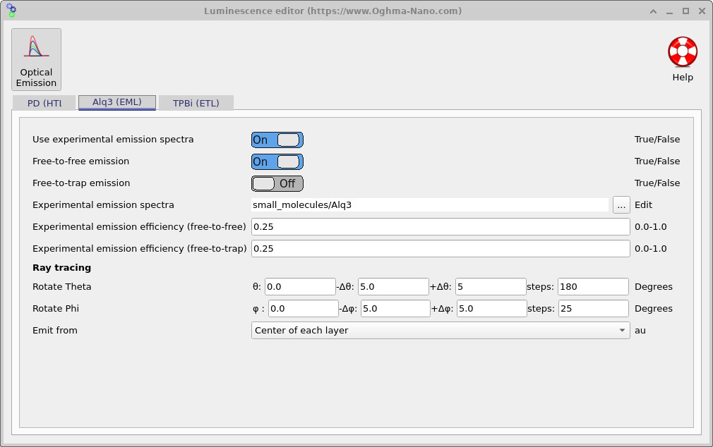
Open the Optical Emission editor shown in ??.
This editor controls the optical emission properties of the OLED layers. In this example the Alq3 emissive layer uses experimentally measured emission spectra.
The transfer matrix solver emits photons from the emissive layer and then calculates how these photons propagate through the multilayer structure.
The angular ray-tracing settings define the angular resolution used when calculating photon propagation and escape probability.
Because the OLED cavity strongly modifies the angular distribution of emitted photons, accurate angular sampling is important when calculating outcoupling efficiency.
6. Optical mesh configuration
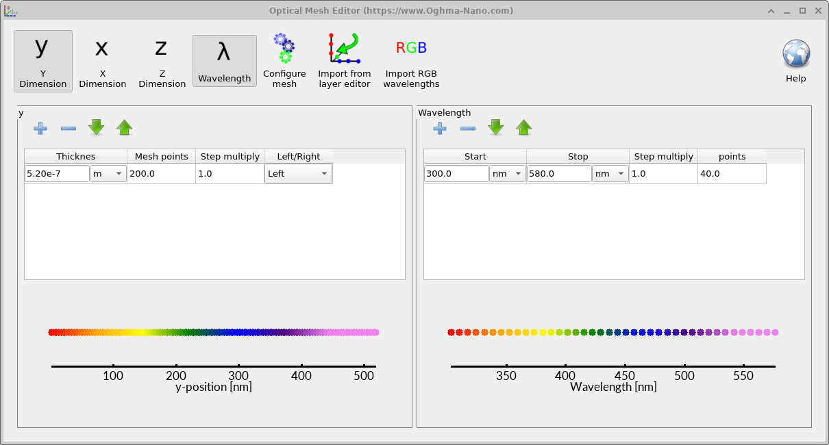
Open the Optical mesh editor shown in ??.
The wavelength mesh controls the spectral range and wavelength resolution used during the OLED outcoupling simulation.
In this example the wavelength range spans approximately 300-580 nm, covering the emission range of the Alq3 emissive material.
Increasing the wavelength resolution improves spectral accuracy, although at the expense of additional computational time.
7. Photon-density distribution
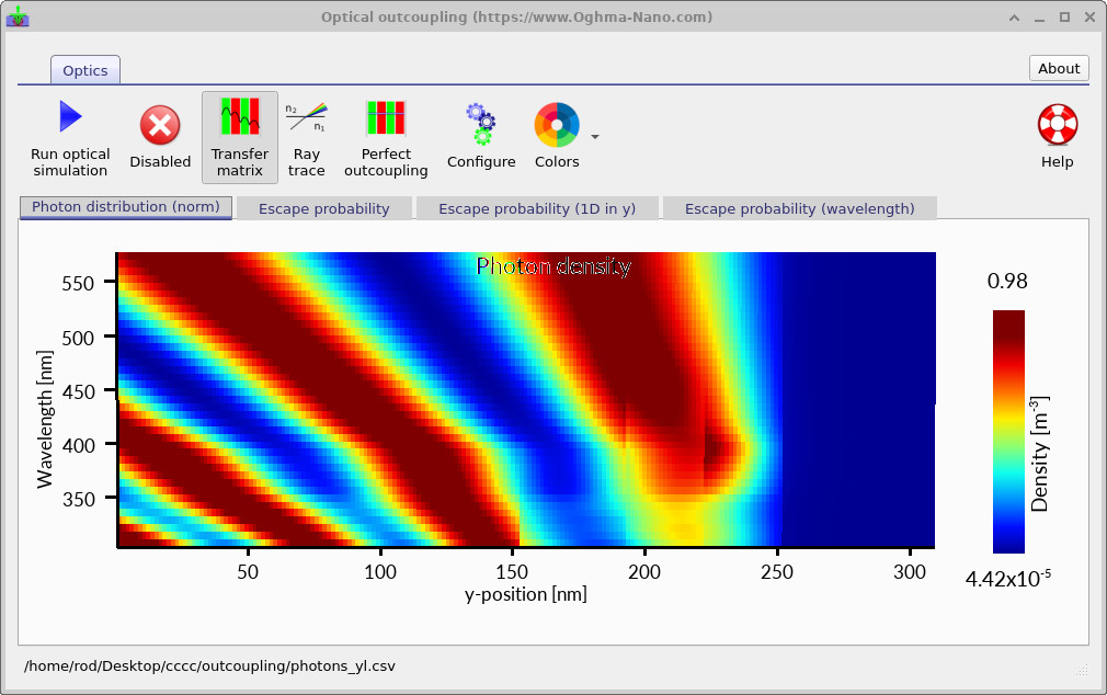
Run the optical outcoupling simulation by pressing the Run optical simulation button.
After the simulation completes, the photon-density map shown in ?? will appear.
The horizontal axis corresponds to position inside the OLED, while the vertical axis corresponds to wavelength.
Bright regions correspond to wavelengths and positions where the optical electric field is enhanced by cavity resonances. Strong standing-wave patterns can be observed throughout the OLED structure due to repeated reflections between the metallic cathode and transparent anode.
These standing-wave patterns strongly influence where photons accumulate inside the device and determine how efficiently photons escape into free space.
8. Photon escape probability
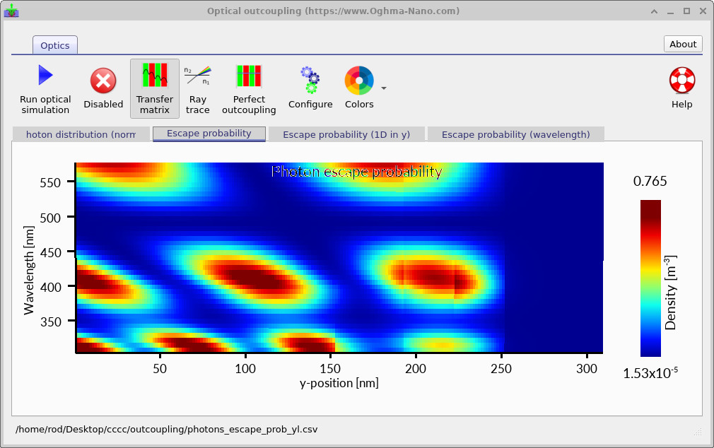
Selecting the Escape probability tab produces the wavelength- and position-dependent escape-probability map shown in ??.
This plot shows the probability that photons generated inside the OLED escape from the device into free space.
The escape probability varies strongly with both wavelength and position because the OLED behaves as a resonant optical cavity.
At certain wavelengths the optical cavity enhances outcoupling, while at other wavelengths photons become trapped inside guided or cavity modes.
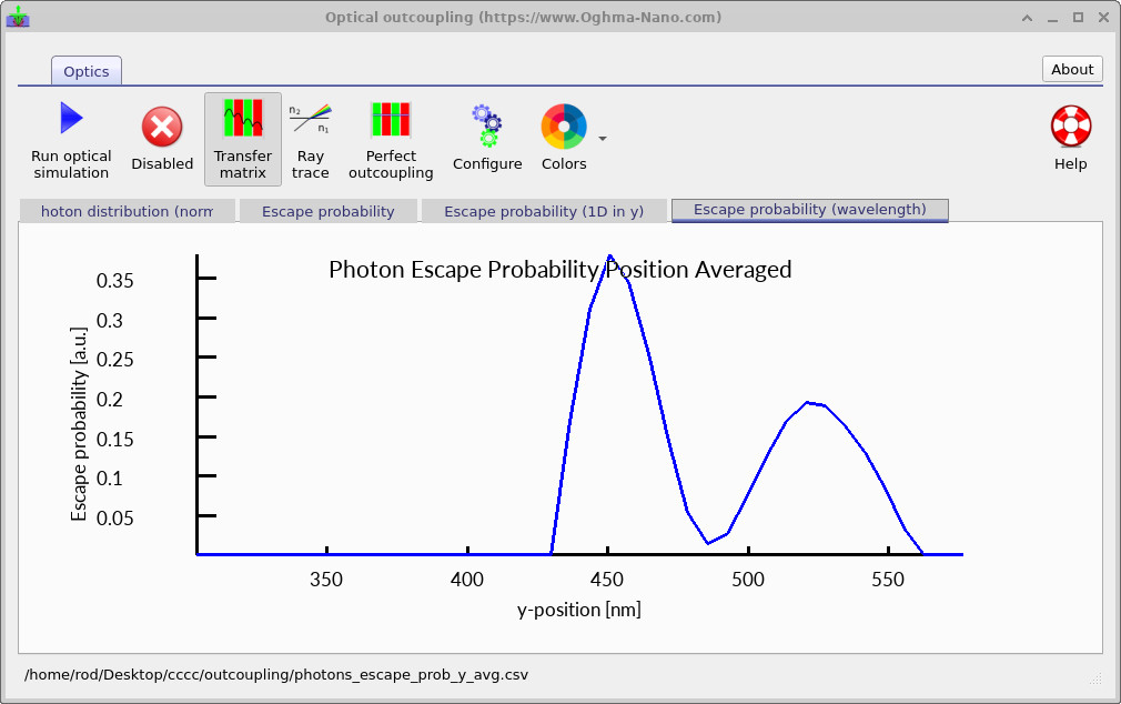
The position-averaged escape probability shown in ?? reveals how outcoupling efficiency varies throughout the visible spectrum.
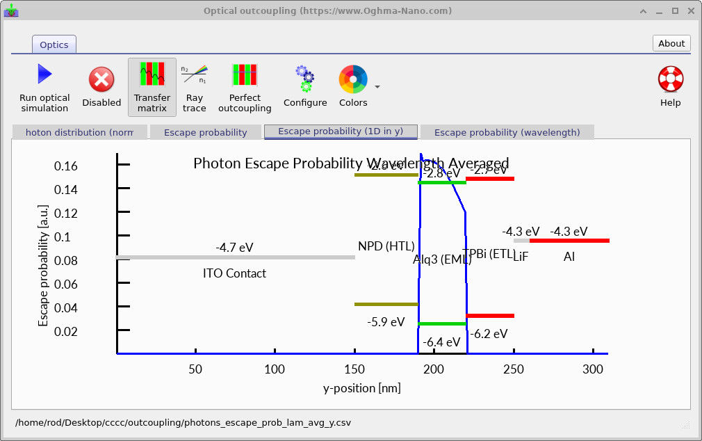
9. Position-dependent escape probability
The Escape probability (1D in y) tab produces the spatially resolved escape-probability profile shown in ??.
This plot shows how efficiently photons escape depending on the position where they are generated inside the OLED.
The highest outcoupling efficiency occurs near the optical field maxima of the cavity mode. Consequently, the precise position of the emissive layer inside the OLED cavity strongly influences the final device efficiency.
In practical OLED design, the emissive layer thickness and cavity position are often tuned carefully to maximise overlap with the optical cavity antinode.
10. Escape probability and device energetics
The optical outcoupling plots can also be displayed together with the OLED energy levels, as shown in ??.
Overlaying the optical field distribution with the electronic structure of the device provides useful physical insight into the relationship between charge recombination and optical outcoupling.
Ideally, electron-hole recombination should occur in regions where the optical escape probability is high. If recombination occurs in regions with poor outcoupling efficiency, a large fraction of photons may remain trapped inside the OLED cavity.
11. Internal emission rather than external illumination
Unlike photovoltaic simulations, OLED optical simulations do not require external illumination. Instead, photons are generated internally within the emissive layer.
The transfer matrix solver then determines how these internally generated photons propagate through the optical cavity and whether they escape into free space or remain trapped inside the device.
This difference fundamentally distinguishes OLED optical simulations from optical absorption simulations in solar cells.
12. Summary
In this tutorial you used the transfer matrix method to simulate optical outcoupling in a multilayer OLED device.
You examined photon-density distributions, wavelength-dependent cavity resonances, and photon escape probabilities throughout the OLED structure.
You also explored how the optical cavity modifies the probability that photons escape from the device into free space.
The transfer matrix method provides a powerful and computationally efficient framework for understanding optical interference, cavity resonances, and outcoupling efficiency in OLED devices.