Perovskite Solar Cell Optical Simulation Using the Transfer Matrix Method (TMM)
Learn how to model optical absorption, interference, reflection, transmission, and charge-carrier generation in multilayer perovskite solar cells using the transfer matrix method (TMM). This tutorial demonstrates how thin-film optical simulations can be used to analyse photovoltaic device performance and estimate the maximum achievable photocurrent in OghmaNano.
1. Introduction
In this tutorial you will simulate the optical behaviour of a multilayer perovskite solar cell using the transfer matrix method (TMM). The simulation calculates the optical field distribution, absorbed photon density, charge-carrier generation profile, and the reflection and transmission spectra of the device.
Optical simulation is often one of the most useful and reliable methods for understanding thin-film solar cells because it depends mainly on the real and imaginary parts of the refractive index, \(n\) and \(k\), which are widely available in the literature and can usually be measured accurately. In contrast, electrical drift-diffusion simulations require many more material and transport parameters that are often difficult to calibrate uniquely. Optical simulations therefore frequently provide more robust physical insight into perovskite and organic photovoltaic devices.
The transfer matrix method solves Maxwell's equations analytically inside each optical layer and matches electromagnetic waves at material interfaces, making the method extremely fast, numerically stable, and well suited to layered photovoltaic structures with strong interference effects. A detailed mathematical derivation is given in Derivation of the transfer matrix method.
In photovoltaic devices, the optical generation profile provides an upper limit for the photocurrent the solar cell can produce. If the optical simulation predicts weak absorption or low generation rates, the device cannot achieve high efficiency regardless of the charge-transport properties. In OghmaNano, the optical generation profile can be coupled directly into the electrical drift-diffusion solver for self-consistent electro-optical simulation. Related examples include anti-reflective coatings, Fabry–Perot cavities, organic solar cells, and OLED optical outcoupling.
2. Making a new simulation
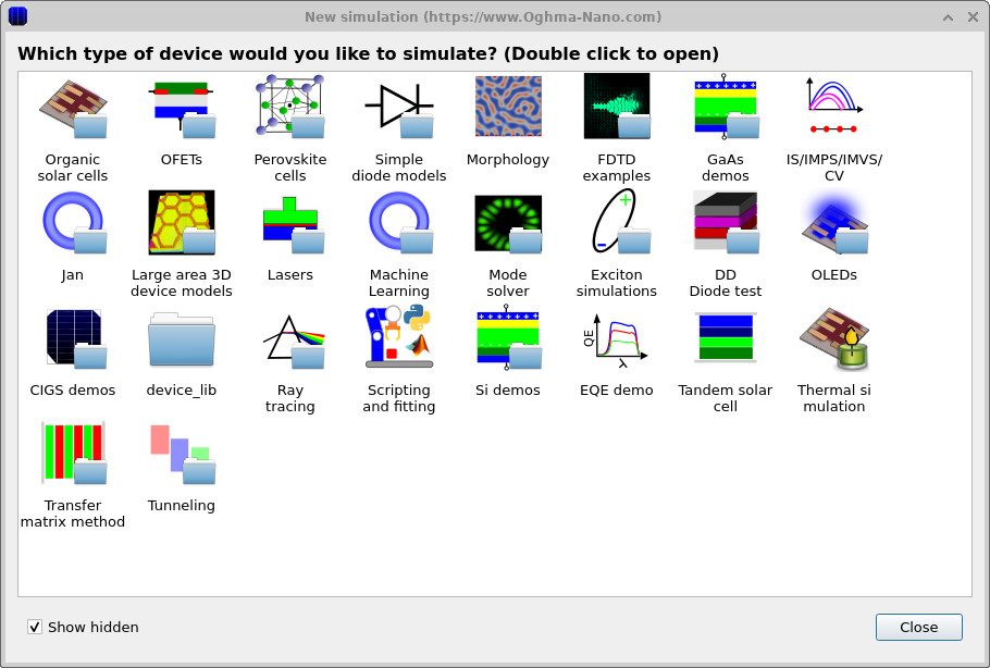
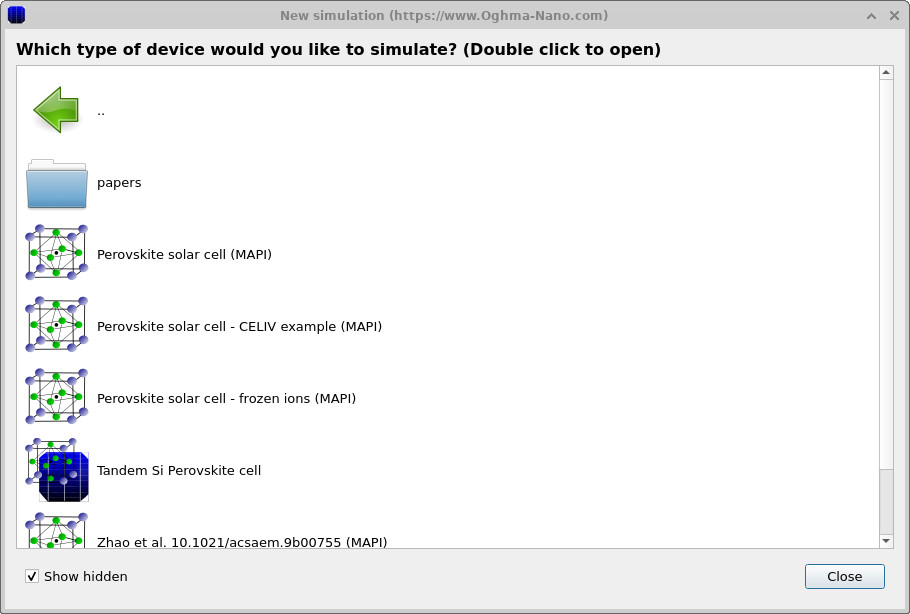
Open the New simulation window and select the Perovskite cells category, shown in ??. Then select the Perovskite solar cell (MAPI) example, shown in ??.
Save the simulation to a suitable directory on disk. Once the example has loaded, the main simulation window shown in ?? will appear.
💡 Tip: For best performance save to a local drive such as
C:\. Simulations stored on network, USB, or cloud folders
(e.g. OneDrive) can run slowly due to heavy read/writes.
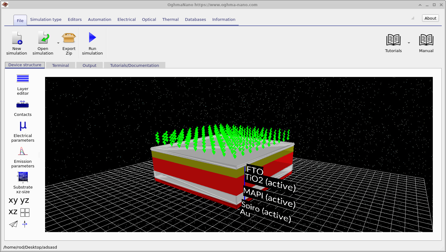
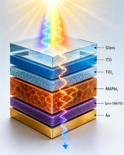
The device consists of a multilayer planar perovskite solar cell including transparent contacts, electron-transport layers, the perovskite absorber, hole-transport layers, and a metallic rear contact. Optical interference between these layers strongly modifies the electromagnetic field distribution inside the device and therefore the local charge-carrier generation rate.
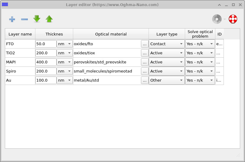
Click on the Layer editor on the left-hand side of the Device structure tab to open the layer editor shown in ??. The device contains a transparent conducting oxide, a TiO\(_2\) electron transport layer, the MAPI perovskite absorber, a Spiro hole transport layer, and a metallic gold contact. The thickness of each layer can be modified directly in the Thickness column.
The optical material assigned to each layer can be changed by clicking on the three-dot button to the right of the material name. This opens the materials database, allowing experimentally measured optical constants \(n\) and \(k\) to be selected for each layer. More information about the materials database and adding new optical materials to OghmaNano can be found here.
3. Opening the transfer matrix solver
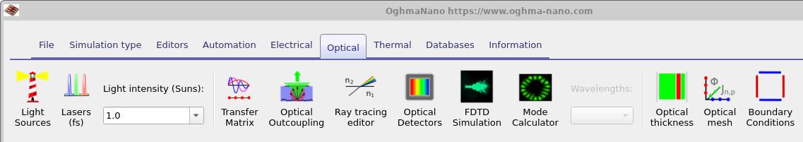
Open the Optical tab shown in ??. This ribbon contains the transfer matrix controls, optical mesh settings, optical detectors, and the light-source editor.
Click the Transfer Matrix button to open the optical simulation editor. Then press the Run optical simulation button (the play button) to execute the optical simulation.
The transfer matrix solver calculates:
- The photon density distribution inside the device.
- The absorbed photon distribution.
- The generation-rate profile.
- The reflected optical power.
- The transmitted optical power.
Because the transfer matrix method solves the layered structure analytically, the simulation usually completes almost instantly.
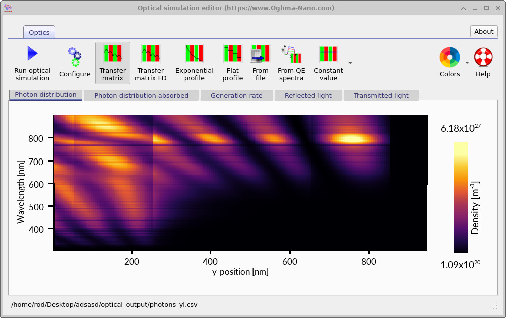
After the simulation has completed, the optical simulation editor will appear with a series of output tabs. The first tab, Photon distribution, displays the photon density inside the device as shown in ??.
The horizontal axis corresponds to position inside the device, while the vertical axis corresponds to wavelength. Bright regions correspond to high optical field intensity. The vertical boundaries visible in the plot correspond to the different layers of the device where the refractive index changes. Interference between forward- and backward-propagating electromagnetic waves produces standing-wave patterns inside the multilayer stack.
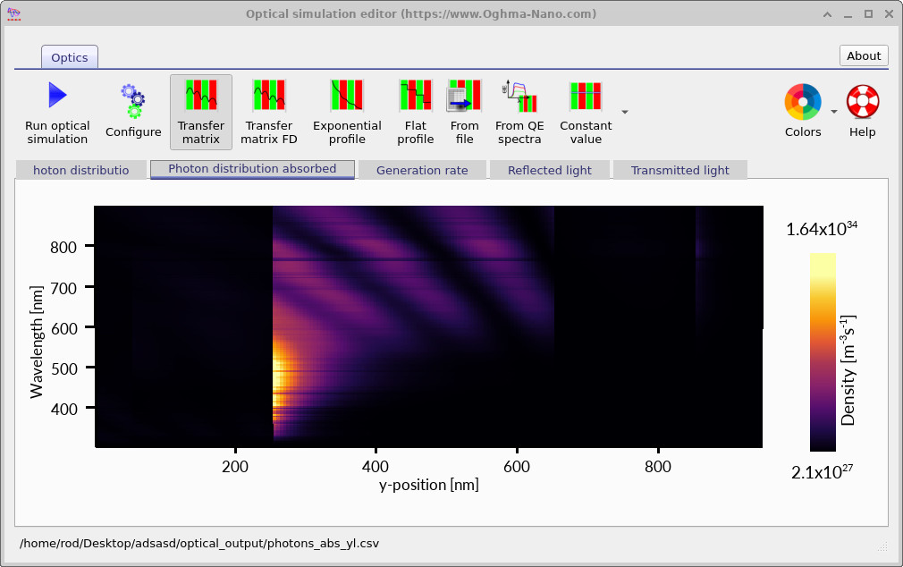
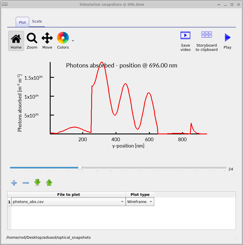
Selecting the Photon distribution absorbed tab produces the absorbed-photon map shown in ??. This plot shows where photons are actually absorbed inside the device, which differs from the total photon density distribution.
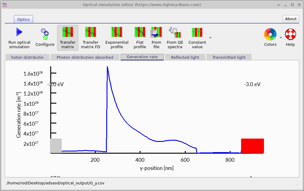
The local optical absorption rate is given by \[ G_{\mathrm{opt}}(y,\lambda)=\alpha(y,\lambda)\,\phi(y,\lambda) \] where \(\alpha\) is the optical absorption coefficient and \(\phi\) is the photon flux density. Optical absorption occurs primarily inside the perovskite absorber layer where electron-hole pairs are generated.
At shorter wavelengths the absorption coefficient is large, causing the optical field to decay rapidly near the front interface. At longer wavelengths the absorption decreases, allowing photons to penetrate more deeply into the structure. These figures therefore show the optical absorption profile as a function of both wavelength and position inside the device.
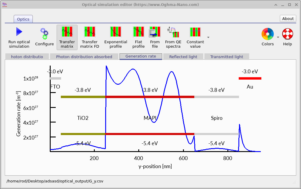
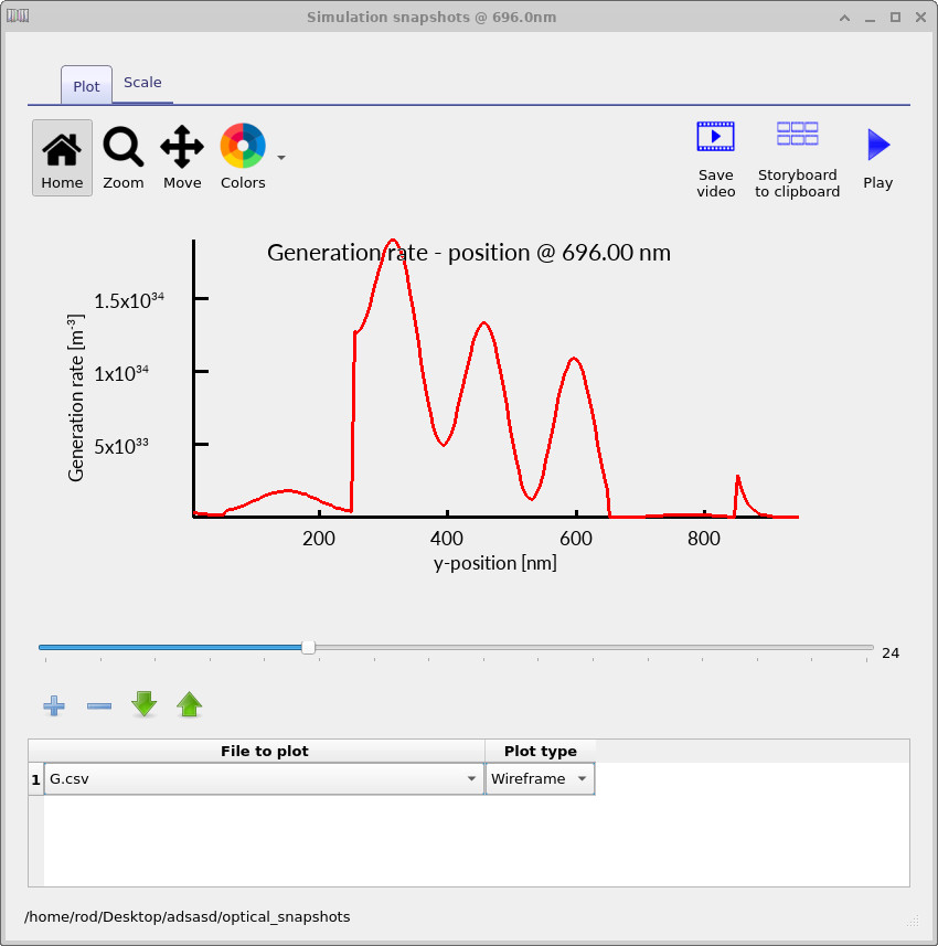
In many cases it is useful to compress the wavelength dependence into a single spatial profile. This can be viewed using the Generation rate tab, where the total charge-carrier generation rate integrated over wavelength is plotted as a function of position within the perovskite device.
4. Reflection and transmission spectra
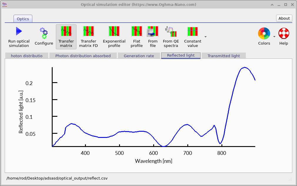
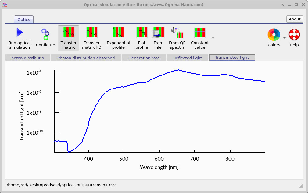
The reflected optical power is shown in ??, while the transmitted optical power is shown in ??. These spectra are often one of the most useful methods for calibrating optical simulations against experimental measurements because reflection and transmission can usually be measured accurately using relatively simple spectroscopic techniques.
Reflection losses reduce the amount of light coupled into the active layer, while transmitted light corresponds to photons passing entirely through the device without being absorbed. In high-performance photovoltaic devices the goal is normally to minimise both quantities so that the majority of incident photons are absorbed inside the active region and converted into charge carriers.
Reflection and transmission spectra also provide direct physical insight into the optical behaviour of the multilayer stack. Sharp oscillations in the spectra are often signatures of thin-film interference, optical cavity effects, or layer-thickness resonances. Small changes in layer thickness or refractive index can substantially shift these features, making optical spectra highly sensitive probes of device structure.
The transfer matrix method is therefore particularly useful for optimising layer thicknesses, refractive-index profiles, and anti-reflective coatings in order to maximise optical absorption and photocurrent generation in thin-film solar cells.
In optical simulations the incident optical power is distributed between reflection, transmission, and absorption inside the device. Neglecting numerical error, energy conservation requires \[ R(\lambda)+T(\lambda)+A(\lambda)=1 \] where \(R\) is the reflected optical power, \(T\) is the transmitted optical power, and \(A\) is the absorbed optical power at wavelength \(\lambda\). This relation is extremely useful when validating transfer matrix simulations because it provides a direct consistency check on the calculated optical spectra.
5. Maximum possible photocurrent
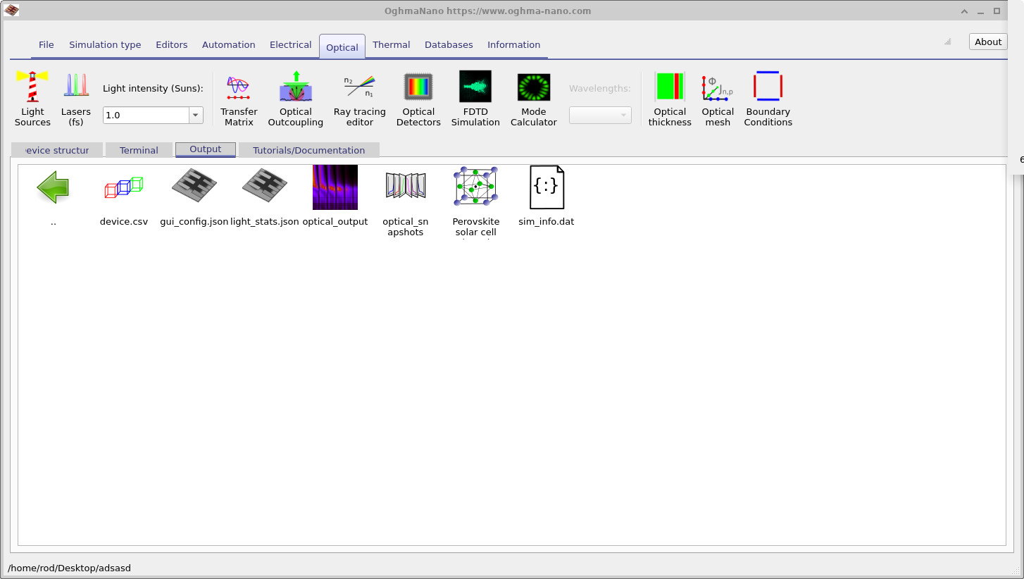
Once the optical simulation has completed, the generated files appear in the Output tab shown in ??. The output directory contains photon-density maps, absorbed-photon distributions, reflection and transmission spectra, and wavelength-resolved generation-rate data.
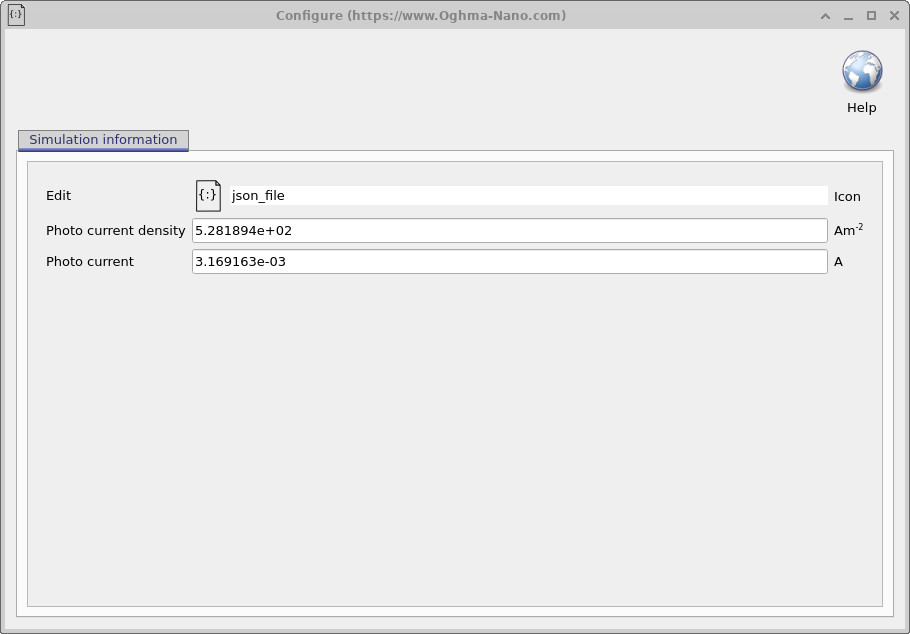
Double-clicking the file
sim_info.dat
opens the simulation information window shown in
??.
This file provides quantitative information about the maximum photocurrent density and photocurrent predicted by the optical simulation.
These values correspond to the maximum possible photocurrent available from optical absorption alone and assume that every generated electron-hole pair is collected successfully without recombination or transport loss. In practice, recombination, trapping, mobility limitations, and imperfect charge extraction reduce the electrical current below this optical upper limit.
The transfer matrix simulation therefore provides a useful first-principles estimate of the maximum achievable photocurrent before electrical drift-diffusion transport and recombination effects are included in the device model.
The total photocurrent available from the optical model is determined by integrating the charge-carrier generation profile throughout the device. In simplified form, the maximum photocurrent density can be written as \[ J_{\mathrm{ph}} = q \int G(x)\,dx \] where \(q\) is the elementary charge and \(G(x)\) is the local volumetric generation rate. This expression illustrates why the spatial distribution of optical generation inside thin-film solar cells is so important when predicting photovoltaic performance.
6. Changing the illumination source
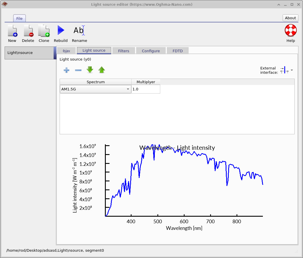
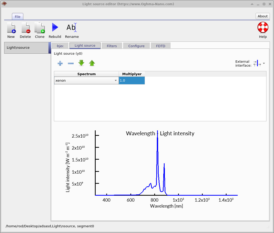
Return to the Optical ribbon shown in ?? and click on Light sources. This opens the light-source editor shown in ??. More information about configuring optical illumination sources can be found here.
By default, the simulation uses the AM1.5G solar spectrum. Notice that the spectrum currently extends only to approximately 900 nm. This is sufficient for many perovskite simulations because the perovskite absorber has relatively weak absorption at longer wavelengths and most photocurrent generation occurs in the visible part of the spectrum.
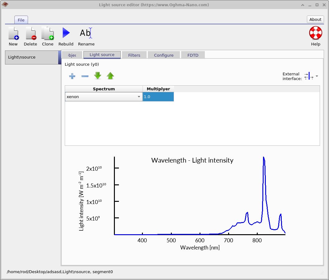
Using the spectrum drop-down menu, change the illumination source from AM1.5G to xenon. The resulting spectrum shown in ?? is again truncated because the optical wavelength mesh is still too short to capture the full xenon emission spectrum.
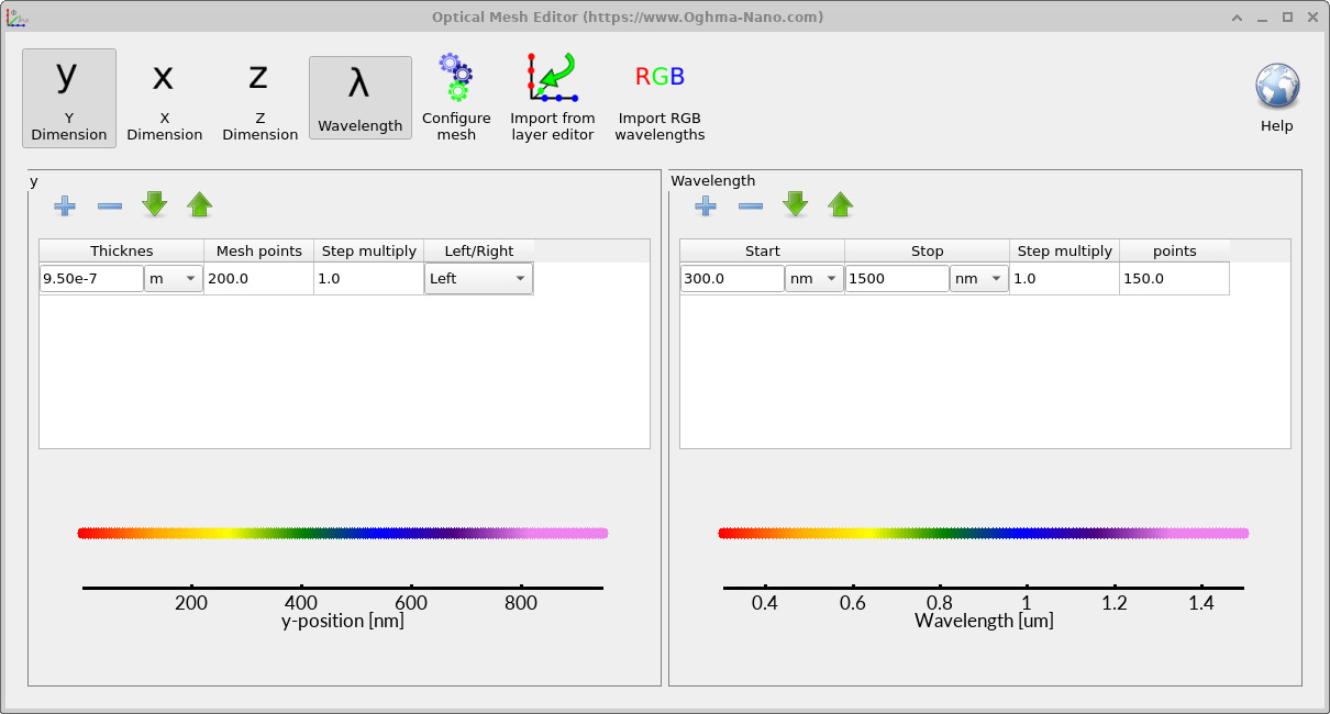
To extend the wavelength range, return to the optical ribbon and open the Optical mesh editor shown in ??. Increase the wavelength stop value to approximately 1500 nm and click Rebuild. Returning to the light-source editor now produces the full xenon spectrum shown in ??.
The optical wavelength mesh controls both the spectral resolution and wavelength range used during the transfer matrix simulation. Choosing an insufficient wavelength range can produce incomplete absorption and generation profiles, particularly when modelling broadband illumination sources or infrared optical behaviour.
After changing the illumination source, rerun the optical simulation. Returning to the Generation rate tab now produces the generation profile shown in ??. Because the xenon lamp has a substantially different spectral distribution compared to AM1.5G sunlight, the optical penetration depth and resulting charge-carrier generation profile inside the device also change significantly.
Correctly matching the illumination spectrum to the experimental light source used in the laboratory is extremely important when comparing simulations with measured photovoltaic performance. In practice, many solar simulators deviate noticeably from the ideal AM1.5G spectrum. OghmaNano therefore also allows custom illumination spectra to be imported through the light-source database editor.
7. Coupling optical generation into the electrical model
The optical generation profile produced by the transfer matrix solver is converted into an electrical generation term inside the drift-diffusion solver.
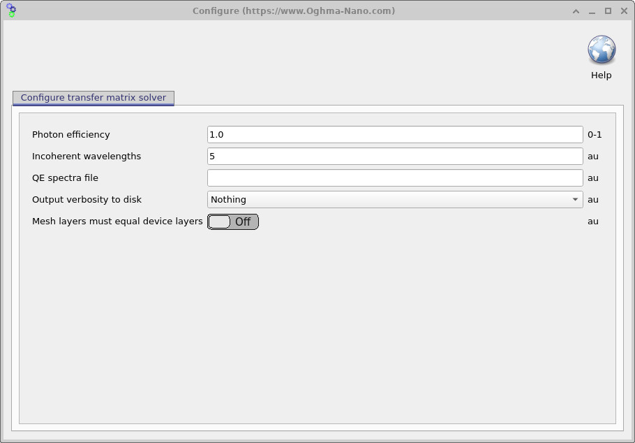
The conversion between the optical generation profile and the electrical drift-diffusion model is controlled by the Photon efficiency parameter shown in ??. This parameter can be accessed by pressing the Configure button inside the optical simulation editor.
The electrical generation rate passed into the drift-diffusion solver is given approximately by \[ G_{\mathrm{dd}}=\eta\,G_{\mathrm{opt}} \] where \(G_{\mathrm{opt}}\) is the generation profile calculated by the optical transfer matrix model and \(\eta\) is the photon efficiency factor.
Physically, \(\eta\) represents the probability that an absorbed photon ultimately produces a free electron-hole pair contributing to the electrical current. In ideal photovoltaic systems this value may approach unity, while in real devices it is often reduced by geminate recombination, incomplete exciton dissociation, parasitic absorption, interfacial losses, or ultrafast recombination processes.
Parameters of this form are widely used in photovoltaic device modelling because optical simulations generally calculate photon absorption rather than the detailed microscopic physics of charge separation. The photon-efficiency factor therefore provides an effective bridge between the optical model and the electrical transport model.
In practice, \(\eta\) can also act as a small fitting parameter when calibrating simulations against experimental devices, particularly if the optical constants \(n\) and \(k\), layer morphology, or interfacial losses are not known perfectly. However, large deviations from unity usually indicate that additional physical mechanisms should be included explicitly in the electrical model rather than absorbed entirely into the efficiency parameter.
8. Examining the optical snapshots
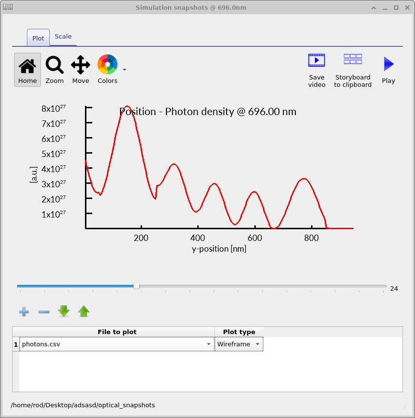
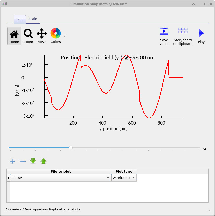
Returning to the Output tab, double-click on the optical_snapshots directory. This opens the optical snapshot viewer, which allows individual optical quantities to be examined at specific wavelengths inside the multilayer device structure.
The slider located below the graph can be used to move between wavelengths, while the drop-down menu at the bottom of the window allows different optical quantities to be selected. These include the photon density, absorbed photon density, optical absorption coefficient, generation rate, and the forward- and backward-propagating electric-field components.
The photon-density plot shown in ?? corresponds to the local electromagnetic field intensity inside the device. Standing-wave interference patterns can clearly be observed due to reflections between interfaces inside the multilayer stack.
The absorbed-photon profile shown in ?? indicates where optical energy is actually absorbed inside the structure. This absorbed optical power is converted into the charge-carrier generation profile shown in ??.
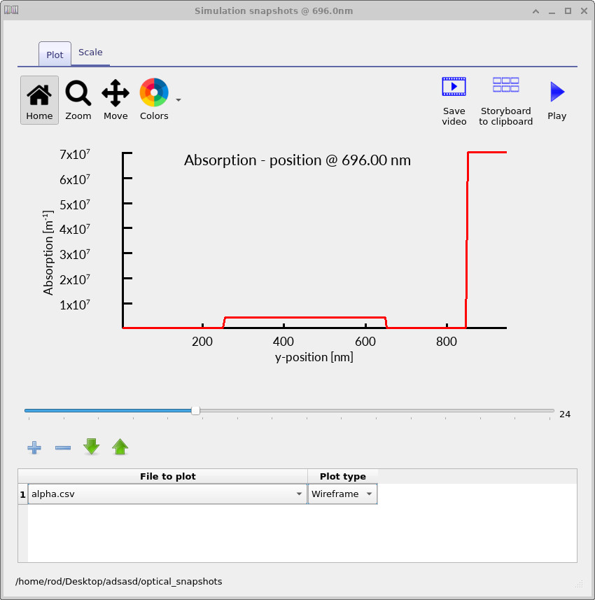
The absorption coefficient profile shown in ?? corresponds to the wavelength-dependent optical absorption coefficient \(\alpha\) of each material layer. Layers with larger values of \(\alpha\) absorb photons more strongly, producing more rapid attenuation of the optical field.
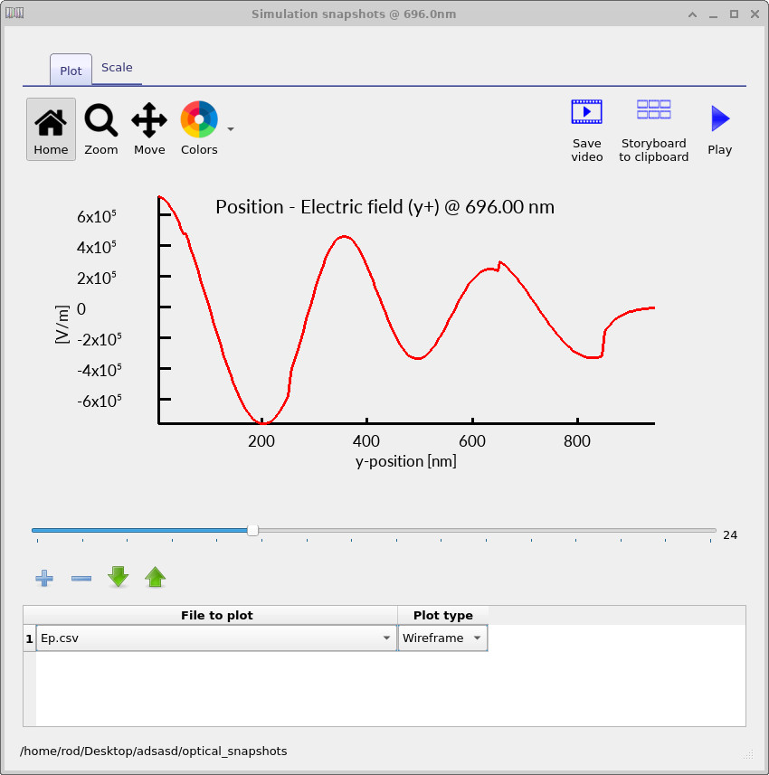
The forward- and backward-propagating electric-field components shown in ?? and ?? correspond to the two counter-propagating electromagnetic waves used internally by the transfer matrix method. Interference between these waves produces the standing-wave optical patterns observed throughout the device.
These optical snapshots provide detailed insight into how light propagates, reflects, interferes, and is absorbed inside thin-film photovoltaic structures, making them particularly useful for understanding optical cavity effects and optimising multilayer solar-cell architectures.
9. Summary
In this tutorial you used the transfer matrix method to simulate the optical behaviour of a multilayer perovskite solar cell in OghmaNano. You examined photon-density distributions, absorbed-photon maps, wavelength-dependent generation profiles, reflection and transmission spectra, and maximum photocurrent estimates derived from the optical model.
You also explored how changing the illumination spectrum and optical wavelength mesh modifies the charge-carrier generation profile inside the device. These effects are particularly important when comparing simulations against experimental measurements because thin-film photovoltaic devices are highly sensitive to optical interference, illumination conditions, and layer thickness.
Optical transfer matrix simulations are one of the most powerful tools available for understanding and optimising thin-film solar cells because they require relatively few material parameters while still providing highly reliable physical insight into optical absorption and photocurrent limits. In OghmaNano, the transfer matrix solver forms the optical foundation for coupled electro-optical drift-diffusion simulations, allowing optical generation profiles to be linked directly to charge transport and recombination models.