Organic Solar Cell Optical Simulation Using the Transfer Matrix Method (TMM)
Learn how to simulate thin-film organic solar cells using the transfer matrix method in OghmaNano. This tutorial demonstrates how optical interference, absorption, and multilayer cavity effects influence photon absorption, charge-carrier generation, and the maximum achievable photocurrent in organic photovoltaic (OPV) devices.
1. Introduction
In this tutorial you will simulate the optical behaviour of a thin-film organic photovoltaic (OPV) solar cell using the transfer matrix method (TMM). The simulation calculates the optical field distribution, absorbed photon density, charge-carrier generation profile, and the reflection and transmission spectra of the device. More information about the implementation of the transfer matrix solver in OghmaNano can be found here, while a full derivation of the method is given here.
Optical simulations are often one of the most reliable ways to obtain a first understanding of photovoltaic device performance because relatively few material parameters are required. Only the refractive index \(n\) and absorption coefficient \(\alpha\) of each layer are needed, both of which are widely available in the literature and can usually be measured accurately. This contrasts with electrical drift-diffusion models, where parameters such as mobility, recombination rates, trap densities, and interfacial properties can depend strongly on operating conditions and are often difficult to determine uniquely.
Organic photovoltaic devices are particularly sensitive to optical interference because the active layers are typically only a few hundred nanometres thick. Reflections at material interfaces produce standing-wave patterns inside the multilayer stack, causing the optical electric field and generation profile to vary strongly with wavelength, layer thickness, and optical constants. The optical model therefore provides direct insight into where photons are absorbed and where charge carriers are generated inside the device.
The transfer matrix method solves Maxwell’s equations analytically within each layer and matches the forward- and backward-propagating electromagnetic waves across interfaces. Because the method makes relatively few assumptions and avoids explicit time propagation, it is computationally efficient and significantly faster than full-wave techniques such as FDTD. Transfer matrix simulations are therefore widely used as a first stage of thin-film solar-cell optimisation before introducing electrical transport and recombination models.
The optical model also provides an upper limit for the achievable short-circuit current density \(J_{SC}\). If the multilayer stack does not absorb light efficiently, then even ideal electrical transport will not produce a high-performance device. Related examples of optical optimisation can be found in the optical filter, anti-reflective coating, Fabry–Perot cavity, perovskite solar cell, and OLED optical outcoupling tutorials.
In OghmaNano, the optical generation profile calculated by the transfer matrix solver can be coupled directly into the electrical drift-diffusion model, allowing optical absorption, charge generation, transport, recombination, and extraction to be simulated self-consistently.
2. Creating the simulation
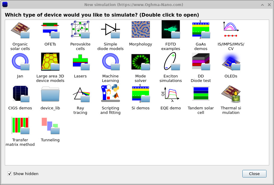
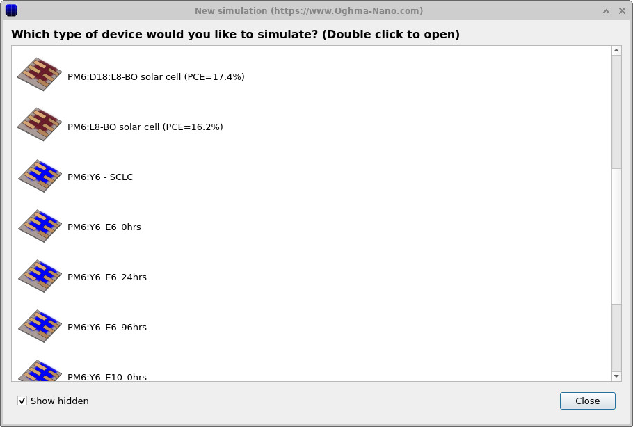
Open the New simulation window shown in ??. Select the Organic solar cells category and then choose the PM6:Y6_E6_0hrs example shown in ??.
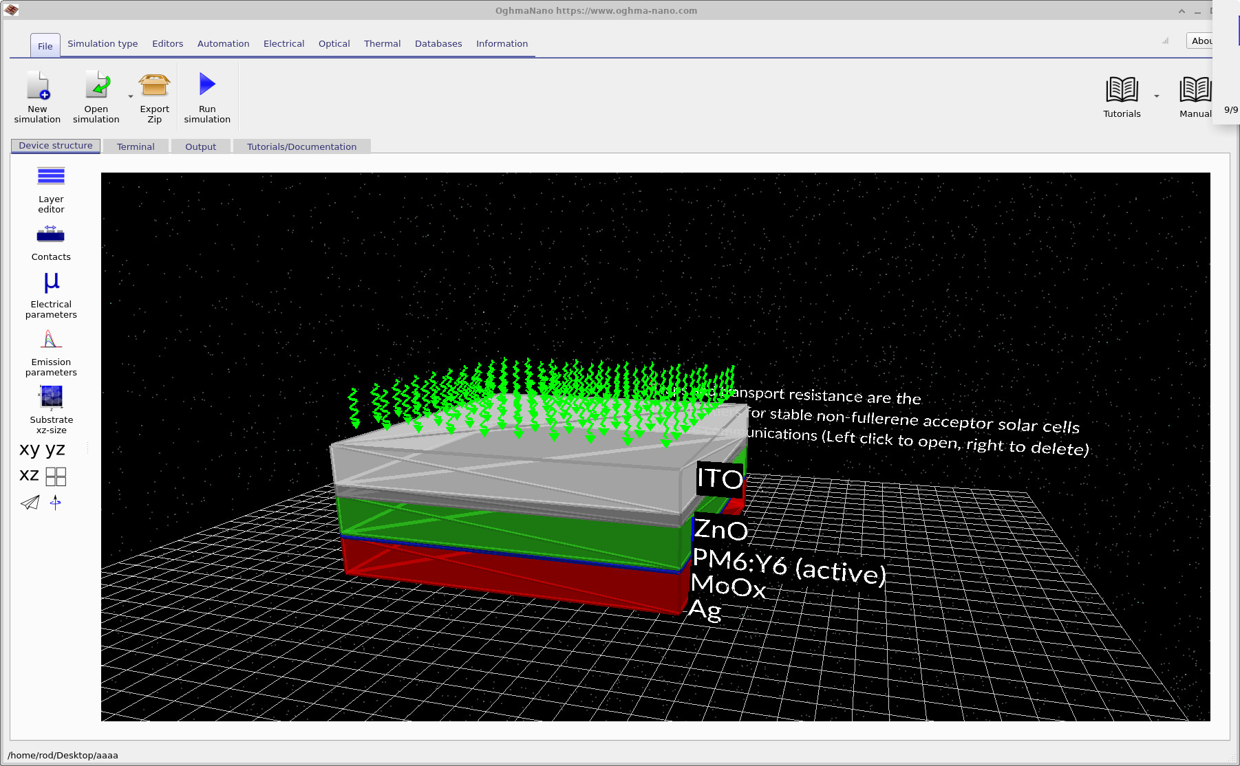
Save the simulation to a suitable directory on disk. Once the simulation has loaded, the main interface shown in ?? will appear.
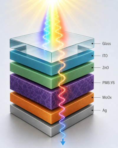
The simulation contains a complete multilayer OPV structure including transparent contacts, transport layers, the PM6:Y6 active layer, and a metallic rear electrode. Because the device thickness is comparable to optical wavelengths, interference effects strongly influence the internal optical field distribution.
3. Examining the device structure
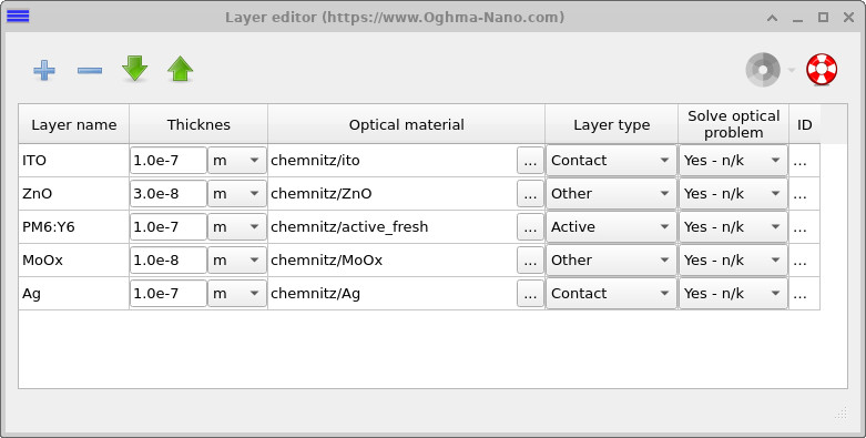
Open the Layer editor from the left-hand toolbar. The multilayer structure shown in ?? will appear.
The device contains an indium tin oxide (ITO) transparent contact, a ZnO electron transport layer, a PM6:Y6 active layer, a MoO\(_x\) hole transport layer, and a silver rear electrode.
Each layer contains experimentally measured optical constants \(n\) and \(k\), allowing wavelength-dependent absorption and interference effects to be simulated accurately.
In thin-film organic solar cells, the optical field often reaches a maximum inside the active layer due to constructive interference. Conversely, destructive interference can suppress the optical field in certain regions. These interference effects strongly influence the final current-voltage characteristics of the device because the charge-carrier generation profile is directly coupled to the optical electric field distribution.
4. Opening the transfer matrix solver
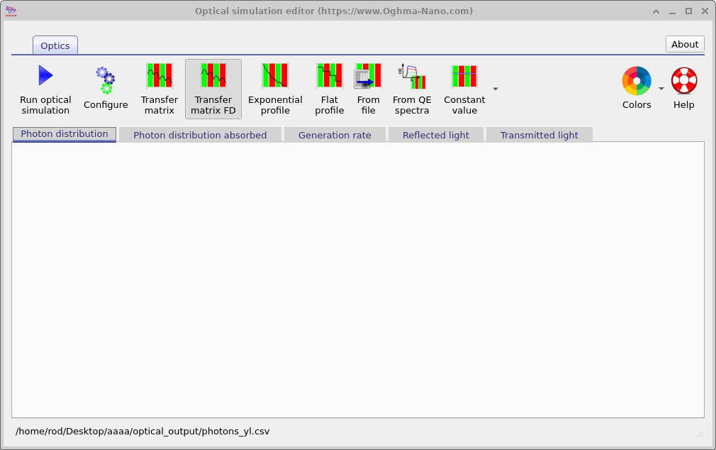
Open the Optical tab shown in ??. This ribbon contains the transfer matrix controls, optical mesh settings, optical detectors, and the light-source editor.
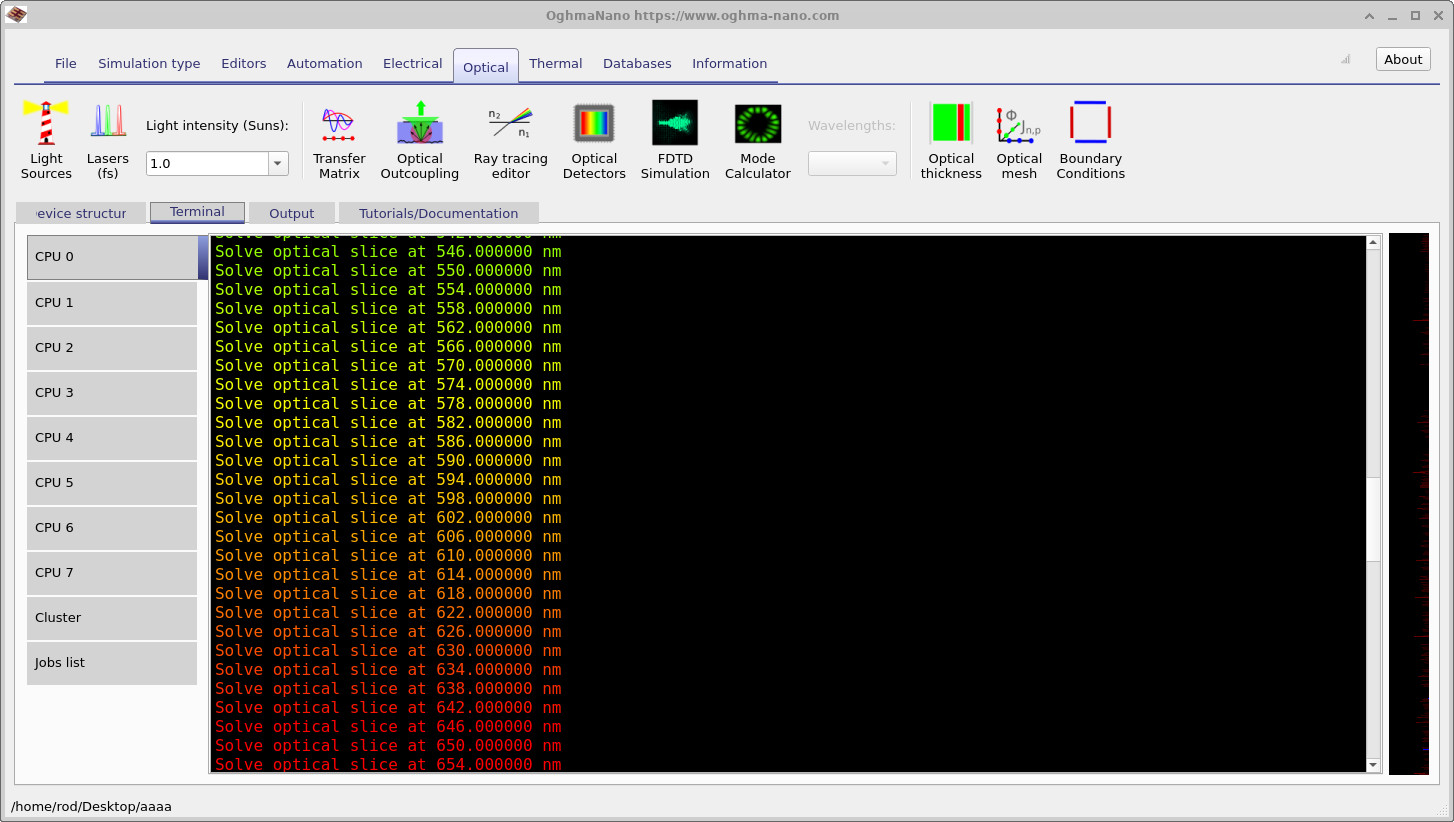
Click the Transfer Matrix button to open the transfer matrix simulation editor shown in ??. To run the optical simulation, press the Run optical simulation button. During execution the terminal output shown in ?? will appear. The solver calculates the photon-density distribution, absorbed-photon density, generation-rate profile, reflection spectrum, and transmission spectrum of the multilayer OPV structure.
Because the transfer matrix method solves the optical problem analytically within each layer, the calculation is extremely fast even for devices containing many wavelengths and multiple absorbing layers.
5. Photon density and absorbed photons
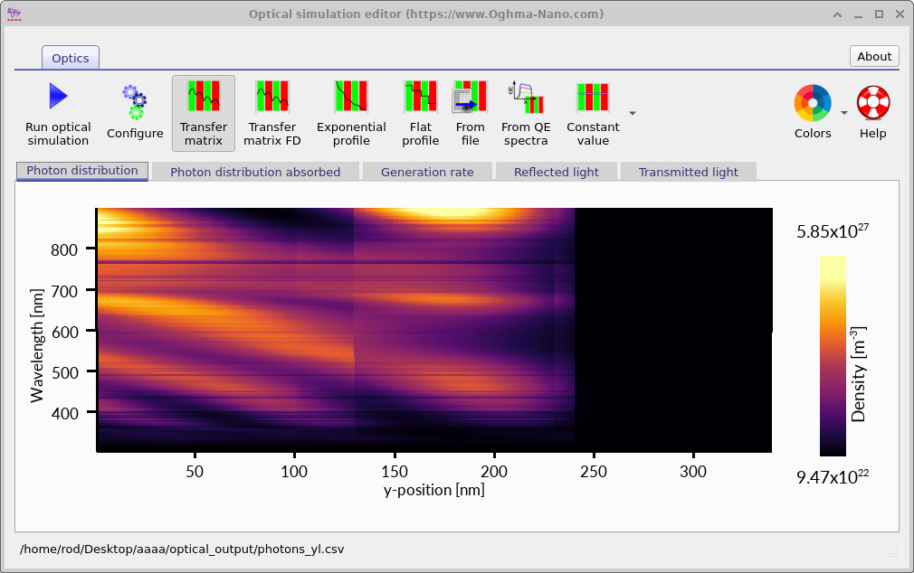
Once the simulation has completed, the photon-density distribution shown in ?? will appear. The horizontal axis corresponds to position inside the device, while the vertical axis corresponds to wavelength. This figure represents the spatial distribution of photons propagating within the multilayer structure, including interference effects arising from reflections at material interfaces.
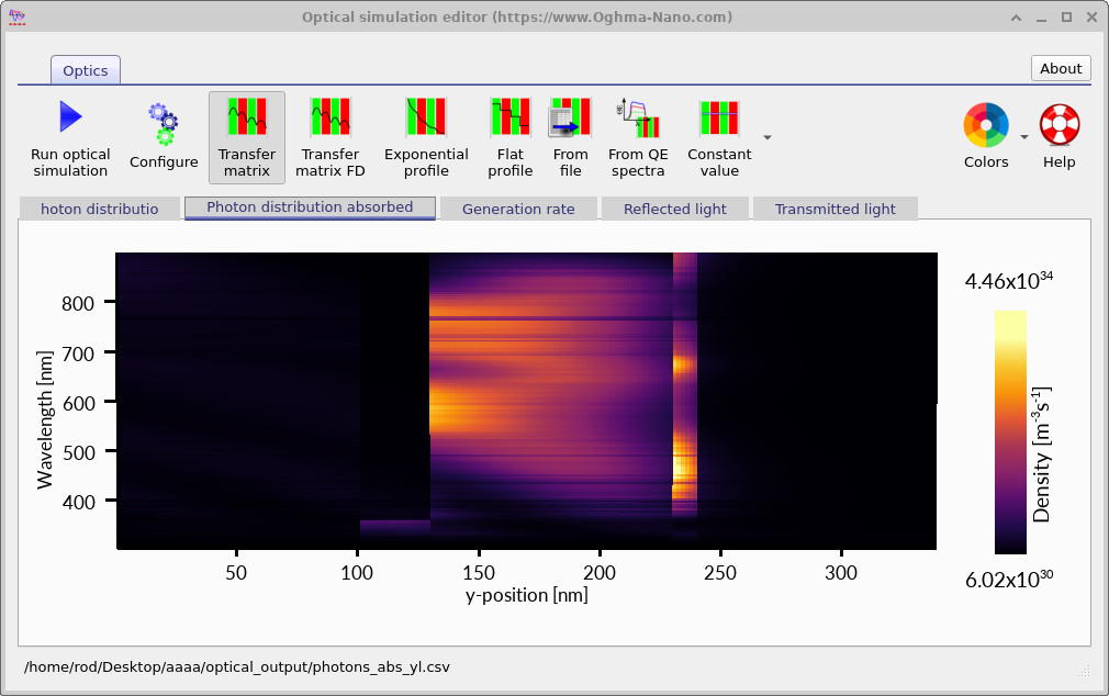
Selecting the Photon distribution absorbed tab produces the absorbed-photon map shown in ??. Unlike the photon-density plot, which shows the total optical field intensity inside the device, this figure shows the photons which are actually absorbed by the material and converted into electron-hole pairs.
The local absorbed-photon density is given by \[ G_{\mathrm{opt}}(x,\lambda)=\alpha(x,\lambda)\,\phi(x,\lambda) \] where \(\alpha\) is the wavelength-dependent optical absorption coefficient and \(\phi\) is the local photon density. Most of the optical absorption occurs inside the PM6:Y6 active layer where the majority of charge generation takes place.
At shorter wavelengths the absorption coefficient is relatively large, causing photons to be absorbed close to the front interface. At longer wavelengths the optical absorption length increases, allowing photons to penetrate more deeply into the active layer before being absorbed. Strong standing-wave patterns are also visible due to coherent interference between forward- and backward-propagating electromagnetic waves inside the thin-film cavity structure.
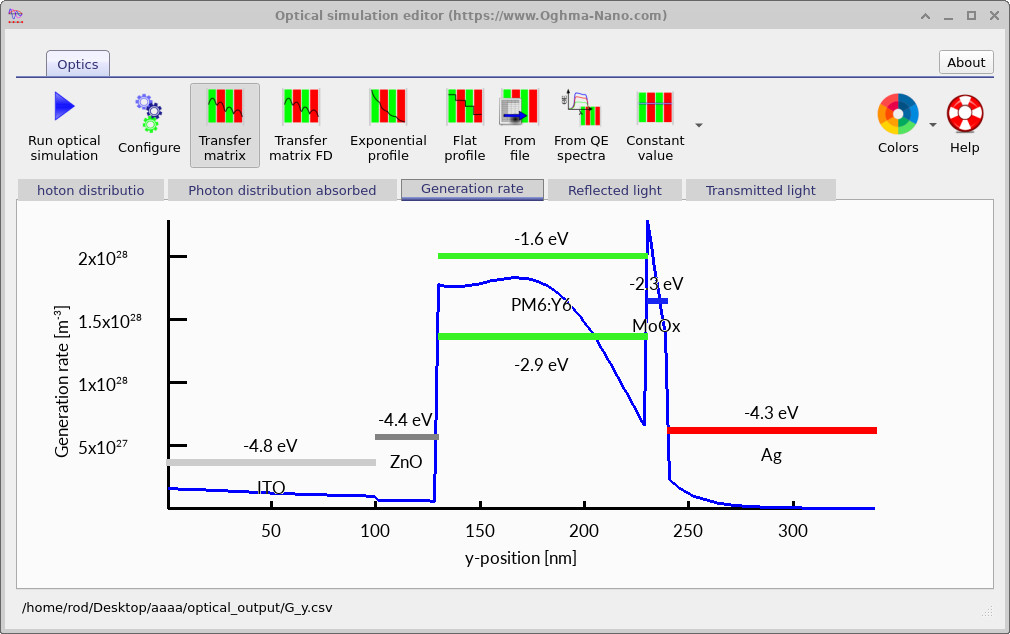
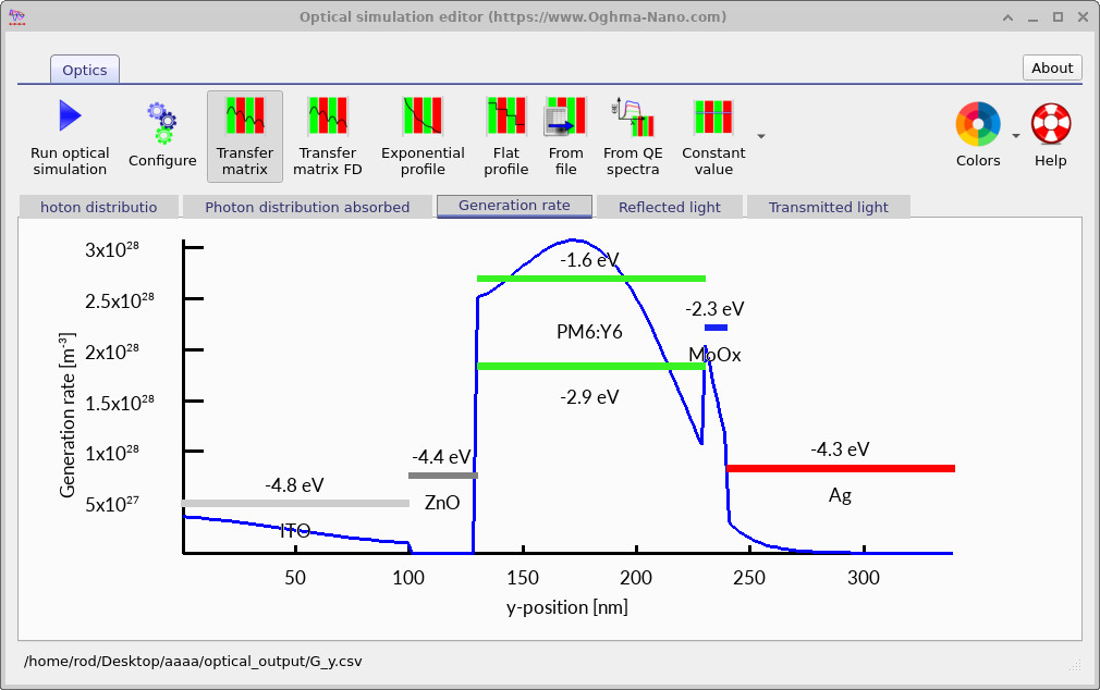
In many cases it is more useful to examine the total generation profile integrated over wavelength rather than viewing the full spectral distribution directly. This can be seen in the Generation rate tab shown in ??, where the total volumetric electron-hole pair generation rate is plotted as a function of position inside the device.
The coloured regions superimposed on the generation-rate plot correspond to the electronic energy levels of the device layers. These energy levels are taken from the materials database and are included primarily as a visual reference for the device structure. They do not directly affect the optical transfer matrix simulation itself. However, for the PM6:Y6 active layer, the energy levels are subsequently used by the electrical drift-diffusion model when charge transport, recombination, and extraction are simulated.
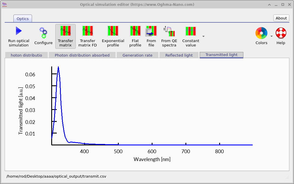
6. Reflection and transmission spectra
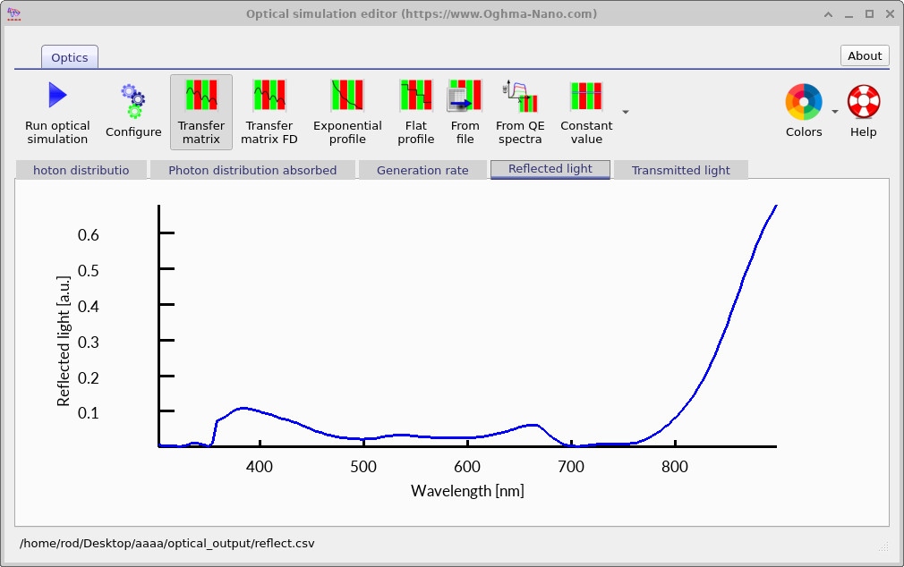
The reflected optical power is shown in ??, while the transmitted optical power is shown in ??. Reflection losses reduce the amount of optical power coupled into the active layer, while transmitted light corresponds to photons leaving the device without being absorbed.
The optical power inside the device is distributed between reflection, absorption, and transmission according to \[ R(\lambda)+A(\lambda)+T(\lambda)=1 \] where \(R\), \(A\), and \(T\) are the reflected, absorbed, and transmitted optical power fractions respectively. This relation follows directly from conservation of energy and provides a useful consistency check for transfer matrix simulations.
At longer wavelengths the transmission approaches zero because the silver rear electrode acts as a strong optical reflector. As a result, most long-wavelength photons are either absorbed within the multilayer structure or reflected back toward the front surface, increasing the effective optical path length inside the active layer.
In practical OPV design, relatively small changes in optical interference, layer thickness, or reflection losses can produce measurable changes in short-circuit current density. Transfer matrix simulations are therefore widely used to optimise cavity effects, optical spacers, and electrode thicknesses in order to maximise absorption inside the active layer.
8. Calculating the maximum possible photocurrent
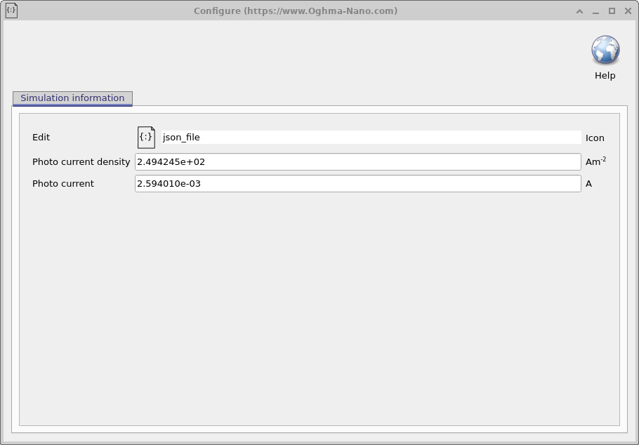
These values represent the maximum possible photocurrent predicted by the optical model under the assumption that every generated electron-hole pair is collected successfully. Recombination, trapping, transport losses, and extraction inefficiencies are not included in this purely optical calculation.
The maximum photocurrent density is obtained by integrating the optical generation rate throughout both wavelength and position, \[ J_{SC,\mathrm{max}} = q \int \int G(x,\lambda)\, d\lambda\, dx \] where \(q\) is the elementary charge and \(G(x,\lambda)\) is the wavelength-dependent volumetric generation rate inside the device.
For well-optimised devices the measured short-circuit current density \(J_{SC}\) is often relatively close to this optical upper limit. Consequently, optical simulations provide an extremely useful first estimate of the achievable device performance. If the optical model predicts a low maximum photocurrent, then no amount of optimisation of the electrical transport model will produce a highly efficient solar cell because the device is fundamentally not absorbing enough light.
9. Changing the illumination spectrum
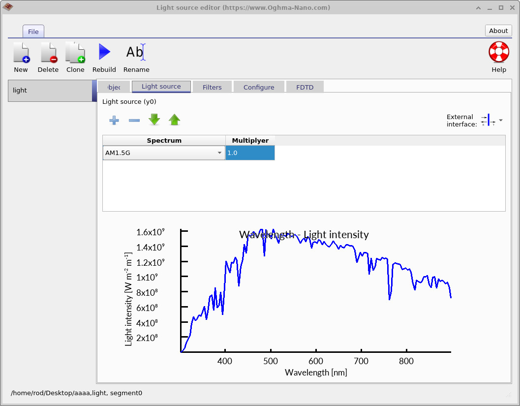
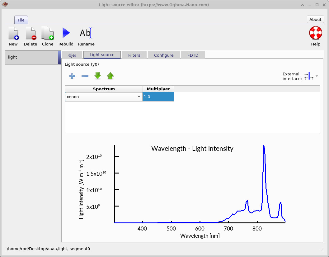

Returning to the Optical ribbon shown in ??, click on the Light sources button, which appears as a lighthouse icon. This opens the light-source editor shown in ??.
By default the simulation uses the standard AM1.5G solar spectrum. Notice that the spectrum is truncated at longer wavelengths. In many OPV simulations this is sufficient because the active layer absorbs relatively weakly in the infrared and most photocurrent generation occurs in the visible spectral range. Restricting the wavelength range also reduces computational cost and improves simulation speed.
In practice, however, many experimental measurements are performed using laboratory solar simulators rather than true AM1.5G sunlight. Xenon lamps are particularly common because their emission spectrum approximately reproduces the visible region of the solar spectrum. Correctly matching the illumination spectrum used experimentally is extremely important because changes in spectral intensity can significantly modify the optical generation profile and measured device performance.
Using the spectrum drop-down menu, change the illumination source to xenon and press Rebuild. The resulting spectrum shown in ?? is again slightly truncated at longer wavelengths because the optical wavelength mesh is still too short to capture the full xenon emission spectrum.
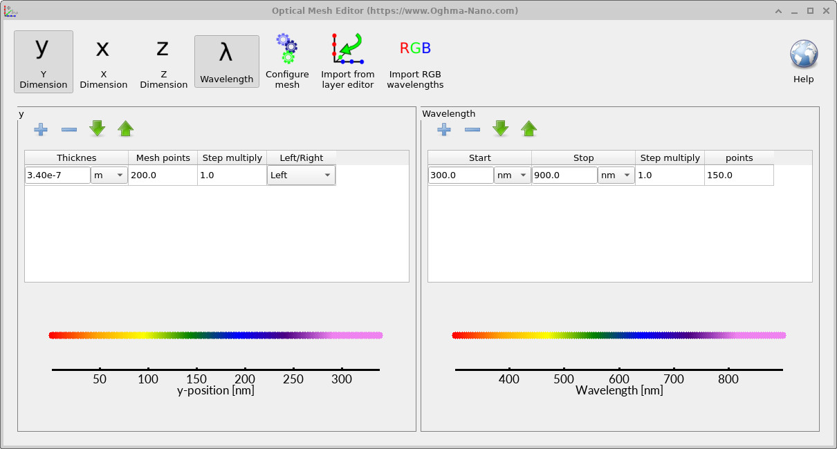
To extend the wavelength range, return to the optical ribbon and open the Optical mesh editor shown in ??. Increase the wavelength stop value to approximately 1500 nm and press Rebuild. Returning to the light-source editor now produces the full xenon spectrum shown in ??.
After modifying the illumination spectrum, rerun the transfer matrix simulation. Returning to the Generation rate tab now produces the profile shown in ??. The spatial distribution of charge-carrier generation is substantially different from the original AM1.5G case because the xenon lamp produces a different spectral intensity distribution and therefore different optical interference conditions inside the multilayer structure.
These effects are particularly important in thin-film organic solar cells because the active-layer thickness is comparable to the optical wavelength. Small changes in illumination spectrum, cavity interference, or absorption length can therefore produce measurable changes in short-circuit current density and overall device efficiency.
9. Coupling optical generation into the electrical model
The absorbed-photon distribution calculated by the transfer matrix solver is converted into an electrical generation term inside the drift-diffusion solver.
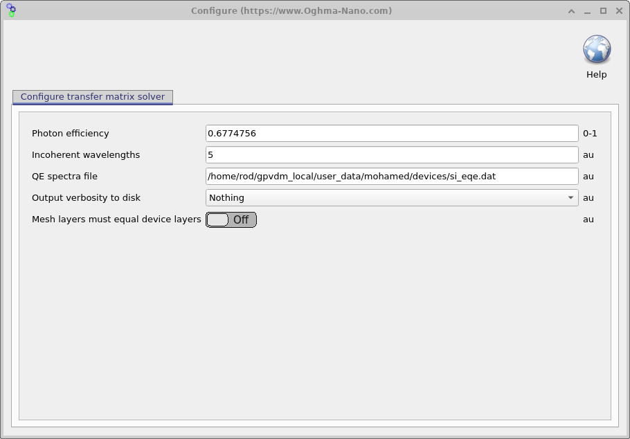
This conversion is controlled by the Photon efficiency parameter shown in ??.
Physically, this parameter represents the probability that an absorbed photon produces a free electron-hole pair contributing to the electrical current.
In organic solar cells this quantity may be significantly below unity because absorbed photons initially form excitons rather than free carriers. Exciton dissociation, geminate recombination, and charge-transfer losses can therefore reduce the final photocurrent substantially.
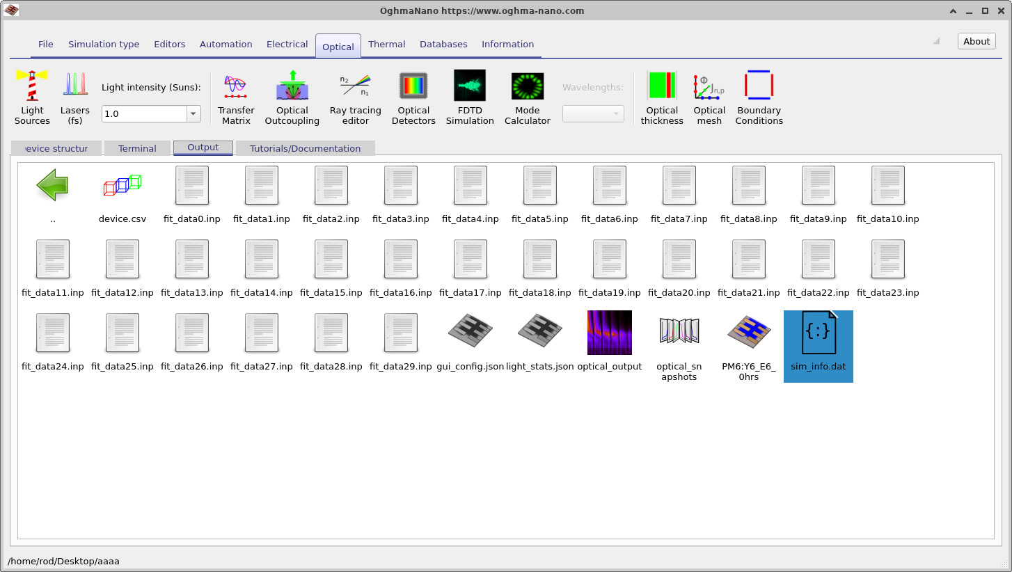
10. Examining the optical snapshots
optical_snapshots folder.
Inside the
Output
tab shown in
??,
double-click on the
optical_snapshots
directory.
This opens the optical snapshot viewer, which allows wavelength-resolved optical quantities to be examined throughout the multilayer OPV structure.
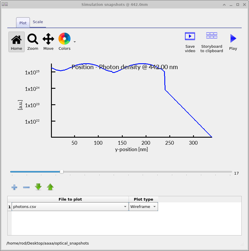
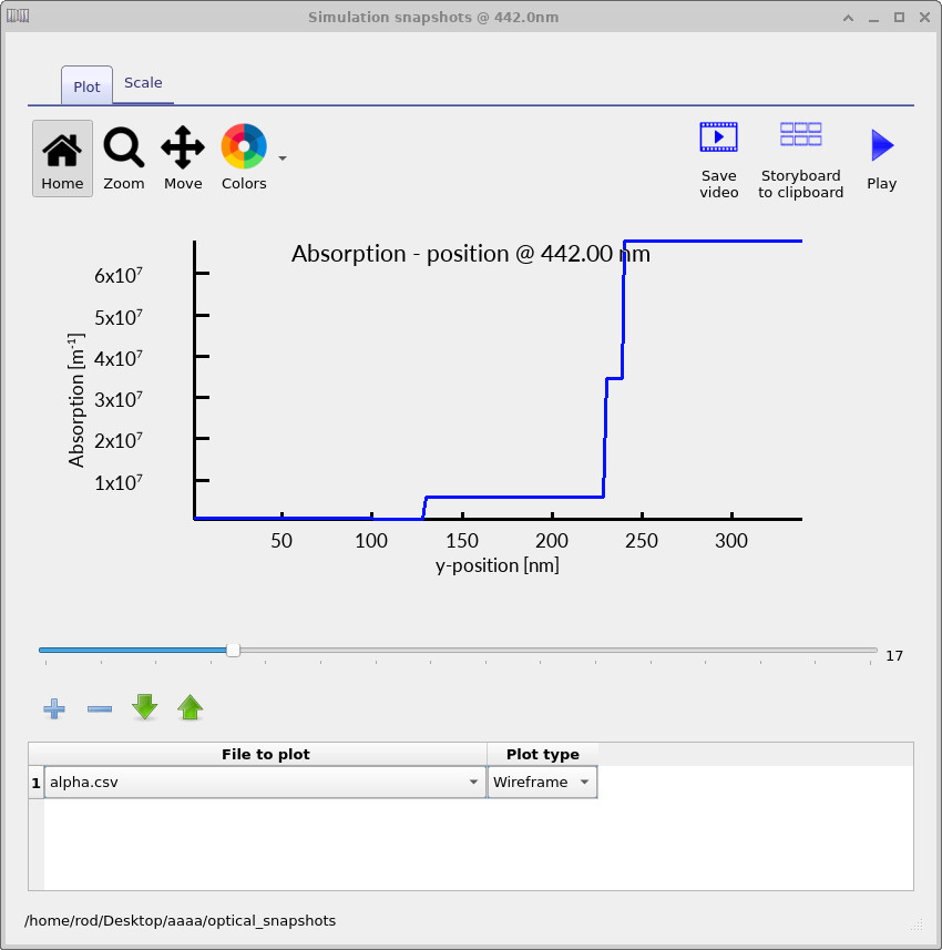
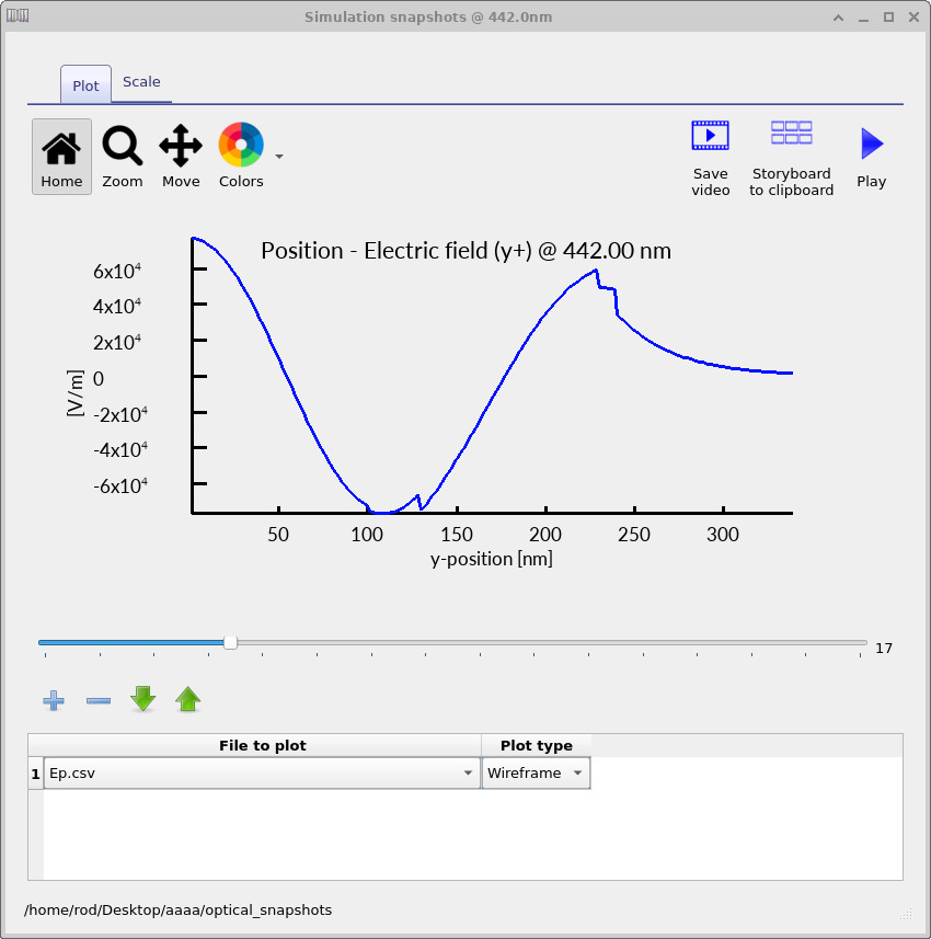
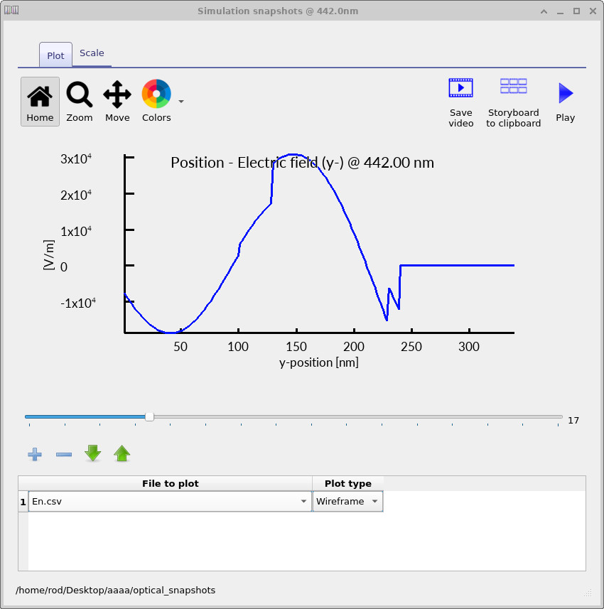
The optical snapshots contain spatial distributions of the photon density, absorption coefficient, forward-propagating electric field \(E^+\), backward-propagating electric field \(E^-\), absorbed-photon density, and generation rate at each wavelength in the optical mesh.
The photon-density distribution shown in ?? illustrates how optical interference modifies the spatial distribution of light inside the device. The absorption profile shown in ?? corresponds to the wavelength-dependent absorption coefficient \(\alpha\) of the multilayer structure.
The electric-field distributions shown in ?? and ?? correspond to the forward- and backward-propagating optical waves calculated by the transfer matrix solver. Interference between these fields produces the standing-wave patterns responsible for the highly non-uniform optical generation profile inside thin-film organic solar cells.
11. Summary
In this tutorial you used the transfer matrix method to model optical absorption, interference, and charge-carrier generation inside a PM6:Y6 organic photovoltaic device. You examined photon-density distributions, absorbed-photon maps, generation-rate profiles, reflection and transmission spectra, and the maximum photocurrent predicted by the optical model.
You also explored how changing the illumination spectrum modifies the optical field distribution and generation profile inside the multilayer structure. These effects are particularly important in thin-film organic solar cells because relatively small changes in optical interference and cavity structure can produce measurable changes in device performance.
The transfer matrix method provides a computationally efficient and physically robust framework for modelling layered photovoltaic devices. Because the method requires relatively few material parameters while still providing detailed insight into optical absorption and photocurrent limits, it is widely used as a first stage of OPV device optimisation before introducing more complex electrical transport and recombination models.
In OghmaNano, the optical generation profile calculated by the transfer matrix solver can be coupled directly into the drift-diffusion model, allowing optical absorption, charge generation, transport, recombination, and extraction processes to be simulated self-consistently.