

Simulating DFB Mirrors and Bragg Gratings with the Finite-Difference Transfer Matrix Method
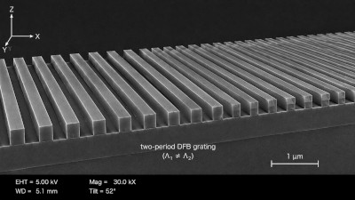
In this tutorial, we use OghmaNano’s finite-difference transfer matrix solver to simulate the reflection, transmission and optical absorption of a distributed feedback (DFB) mirror or Bragg grating. These structures use a periodic modulation of the refractive index to produce strong, wavelength-selective reflection through coherent distributed scattering. In our previous optical filter tutorial, the optical structure was defined through the device epitaxy; here, we instead use Lua scripting to construct the grating directly, allowing arbitrary optical stacks and geometries to be defined. The scripting system is described in more detail in the step editor and scripting documentation. We then examine how a two-period DFB grating determines the resulting reflection, transmission and absorption spectra.
1. Background
Unlike a metallic mirror, which reflects light at a single interface, a DFB mirror reflects light through repeated scattering from a periodic structure (see ??). When the grating period satisfies the Bragg condition, the reflected waves add in phase to produce a strong reflection band, or stop band. The position and width of this band are controlled mainly by the grating period, refractive-index contrast and number of periods.
The reflection band of a DFB mirror is centred on the Bragg wavelength \(\lambda_B\), which is set by the grating period \(\Lambda\) and the effective refractive index \(n_{\text{eff}}\) of the mode propagating through the structure,
\[ m\lambda_B = 2 n_{\text{eff}} \Lambda \]where \(m\) is the diffraction order. The strength of the grating is described by the coupling coefficient \(\kappa\), which measures how strongly the forward and backward propagating waves are coupled by the index modulation \(\Delta n\). For a grating with an approximately square index profile,
\[ \kappa \approx \frac{2\,\Delta n}{\lambda_B} \]The peak reflectivity of a uniform grating of length \(L\) then follows from coupled-mode theory as
\[ R = \tanh^{2}(\kappa L) \]so that increasing either the index contrast or the grating length drives the reflectivity towards unity. The width of the stop band scales with the coupling coefficient,
\[ \Delta\lambda \approx \frac{\lambda_B^{2}\,\kappa}{\pi\, n_{\text{eff}}} \]so high-contrast gratings produce broad, strong reflection bands, while weak gratings produce narrow ones. These simple relations are enough to place the stop band and estimate its strength; a full electromagnetic solution is then needed to capture the detailed spectral shape, ripple and out-of-band behaviour.
The classical transfer matrix method assumes a stack of flat, infinitely periodic layers. Real gratings, however, are rarely perfectly periodic. To handle arbitrary, aperiodic or deliberately perturbed structures — such as the two-period grating simulated in this tutorial — OghmaNano projects the transfer matrix formalism onto a finite-difference grid. The optical structure is discretised in space, and the forward and backward field propagation is solved slice-by-slice across the mesh. This finite-difference transfer matrix approach retains the numerical efficiency and stability of the classical transfer matrix method, while allowing any spatial refractive-index distribution to be simulated, including gratings with more than one period, chirp, apodisation or built-in disorder.
2. Getting started
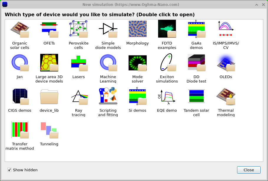
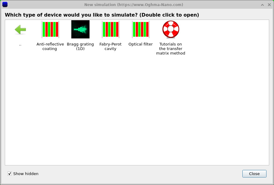
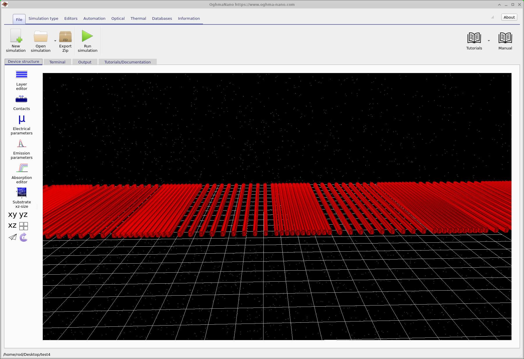
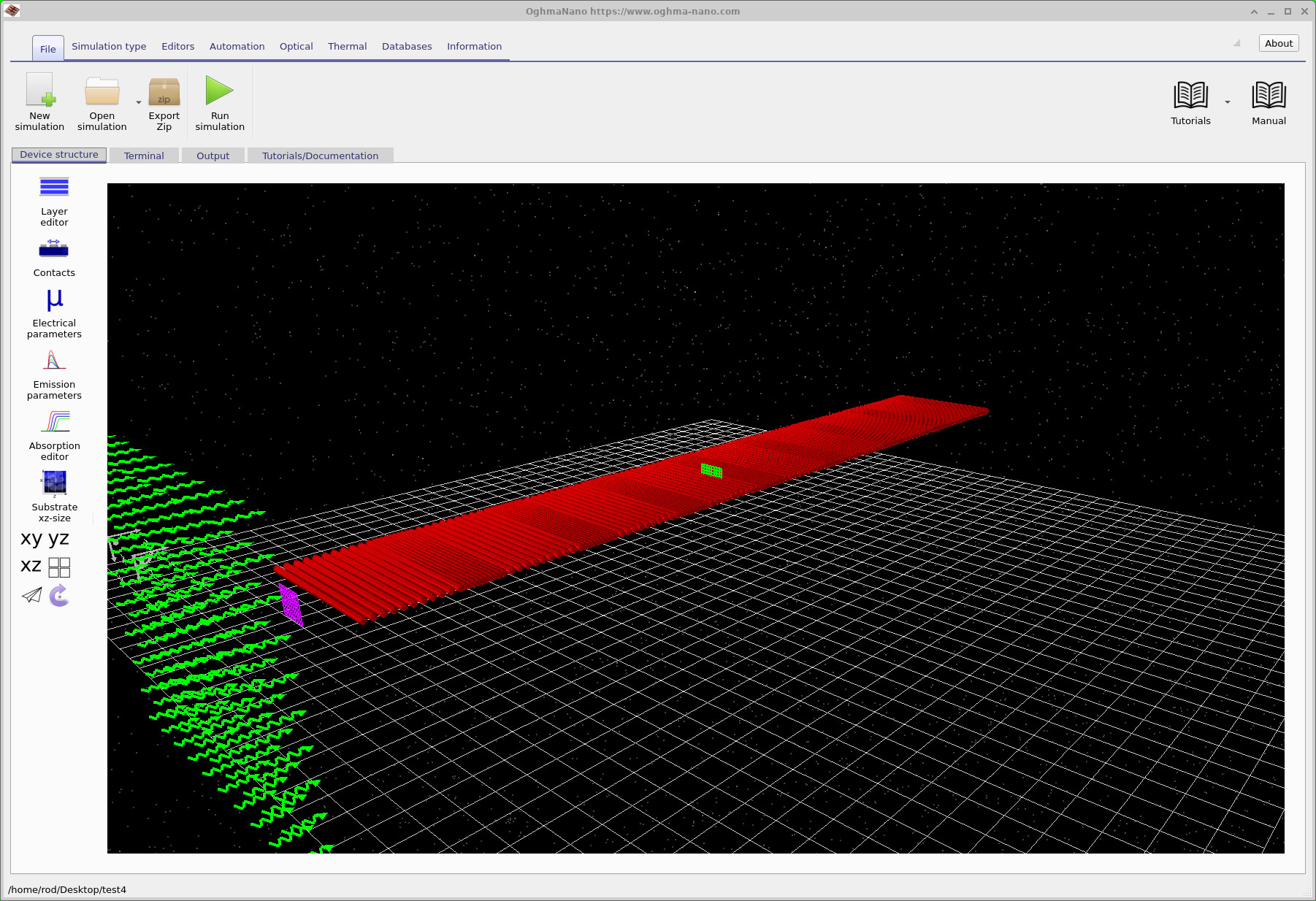
To start your first DFB mirror calculation, open the New simulation window from the File ribbon in the main menu (see ??). Enter the Transfer matrix method group and double-click the Bragg grating (1D) example (see ??), then save the simulation to a folder on your disk. You will then see the main window (see ?? and ??) showing a two-period Bragg grating. The example loads a two-period Bragg grating. The spacing between the narrower gratings is 140 nm, while the spacing between the slightly wider gratings is 218 nm. The grating itself is made of SiO2, while the medium surrounding it is, in this example, air. Once the simulation has opened you can inspect the structure in the main window (see ??).
3. Running the DFB simulation
?? shows the same device
from a slightly different viewpoint.
Click the Run simulation (play) button to compute the spectra
(see ??); once finished, the results
appear in the Output tab
(see ??).
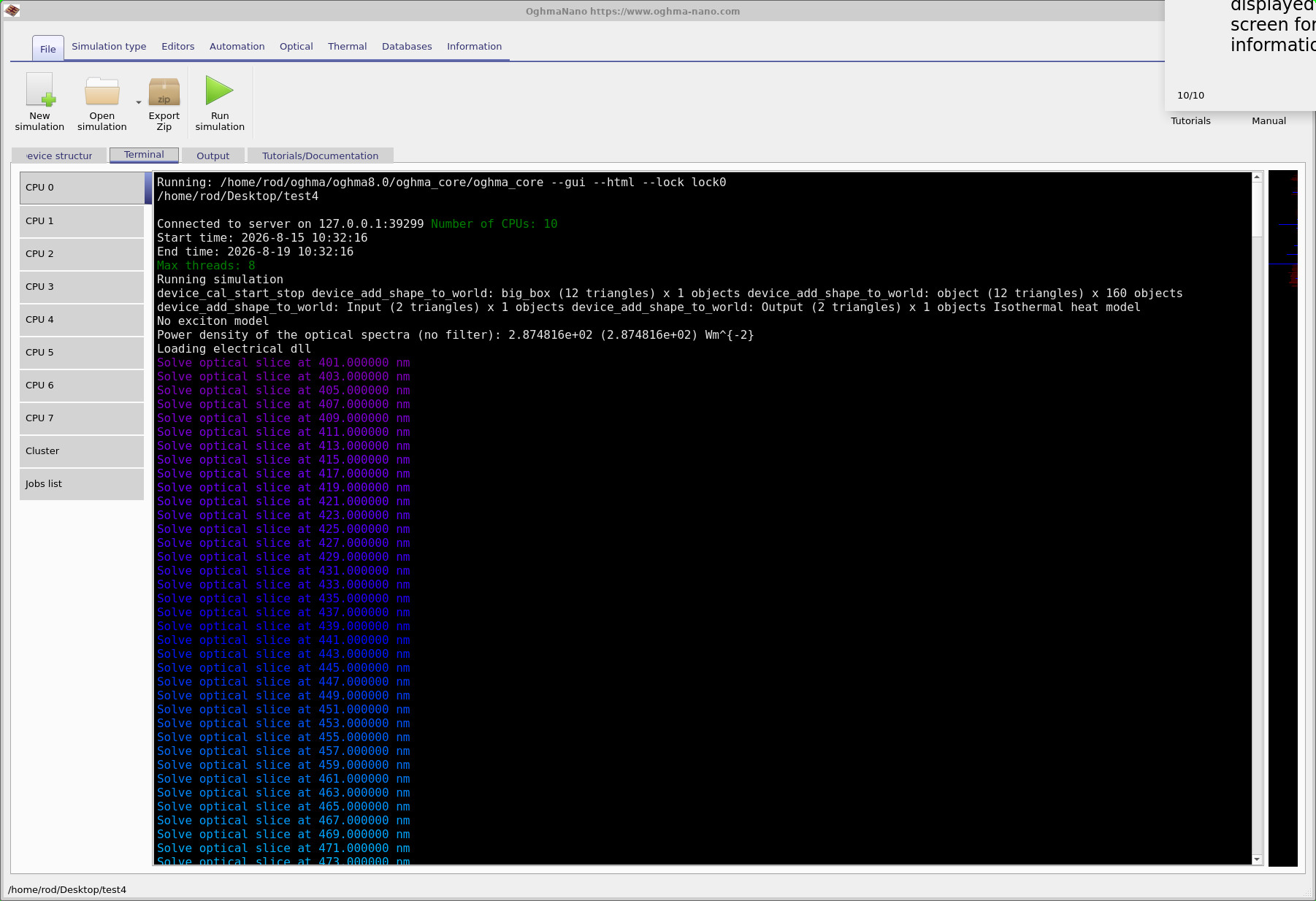
When you click Run simulation, the solver begins stepping
through the optical spectrum, computing one wavelength at a time
(see ??). Each coloured line in the
terminal (Solve optical slice at … nm) corresponds to a different wavelength being solved. As
described above, the method used here is effectively a transfer matrix method projected onto a finite-difference
grid, which is what allows the arbitrary two-period grating to be handled.
3. Examining the Output
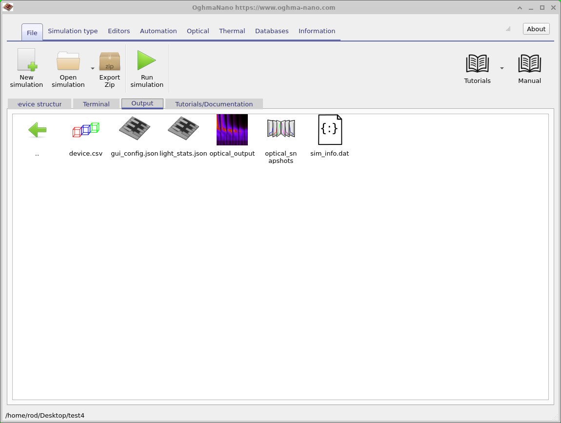
Once the simulation has run, open the Output tab
(see ??) to view the files produced by the calculation.
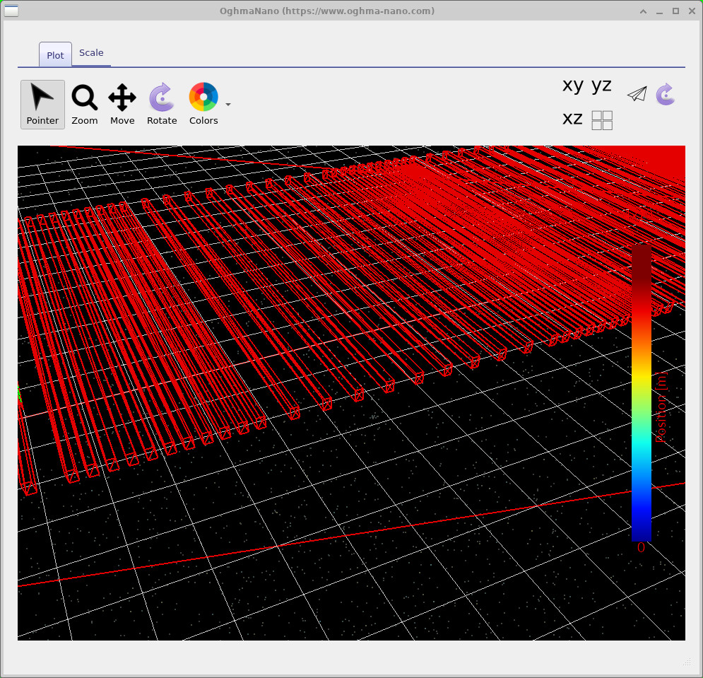
The main outputs used in this tutorial are device.csv, the optical_output folder and the optical_snapshots folder. Start by opening device.csv
(see ??). This shows a three-dimensional mesh of the device as seen by the solver, allowing you to check that the grating geometry has been generated and meshed correctly before examining the optical results.
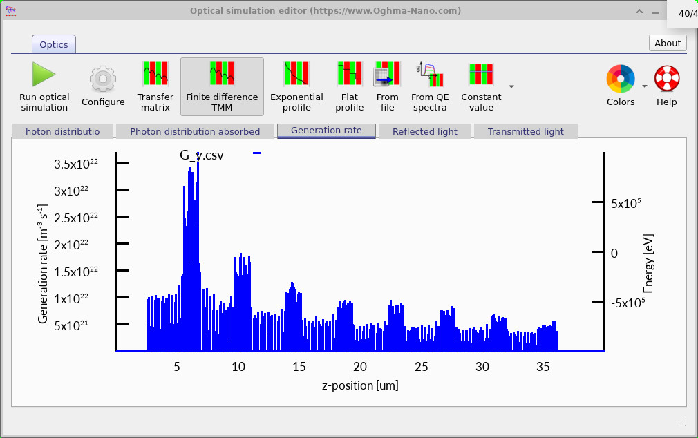
Next, double-click optical_output to open the Optical Simulation Editor. The Generation rate tab (see ??) shows where photons are absorbed within the structure. Regions with little or no absorption correspond mainly to the surrounding air, while stronger absorption occurs within the grating.
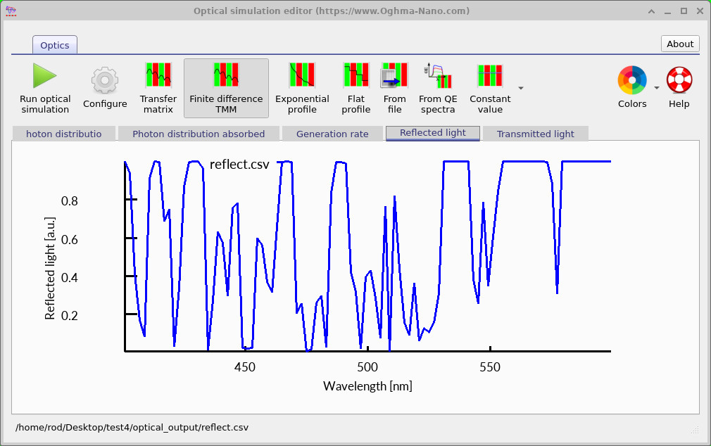
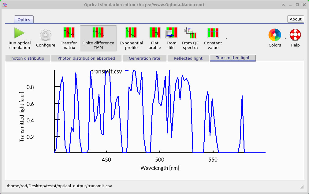
The Reflected light tab (see ??) shows the wavelengths that are reflected by the grating, with clear reflection bands separated by regions of lower reflectivity. The Transmitted light tab (see ??) shows the corresponding transmission spectrum, with high transmission where the reflection is low.
4. Editing the optical materials
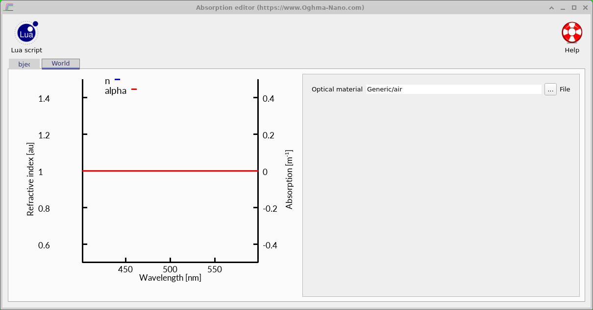
The optical materials used by the grating can be inspected and changed from the Absorption editor,
which is opened from the Device structure tab in the main window. This brings up the absorption
editor (see ?? and
??), which shows the
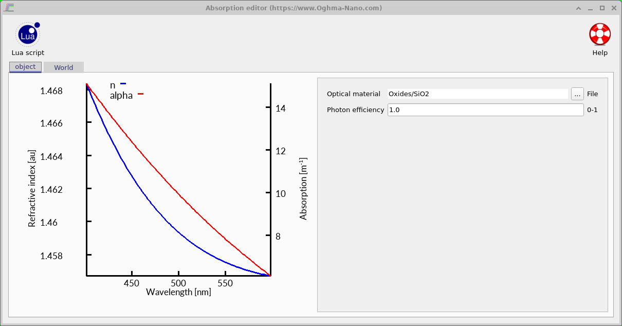
refractive index \(n\) and the absorption \(\alpha\) data of both the SiO2 making up the grating and the
air surrounding it. The object tab
(see ??) displays the material of
the grating itself (Oxides/SiO2), while the World tab
(see ??) displays the
surrounding medium (Generic/air). Here you can change the materials to whichever ones you are
interested in by clicking the … button in the Optical material field.
5. Editing the grating structure
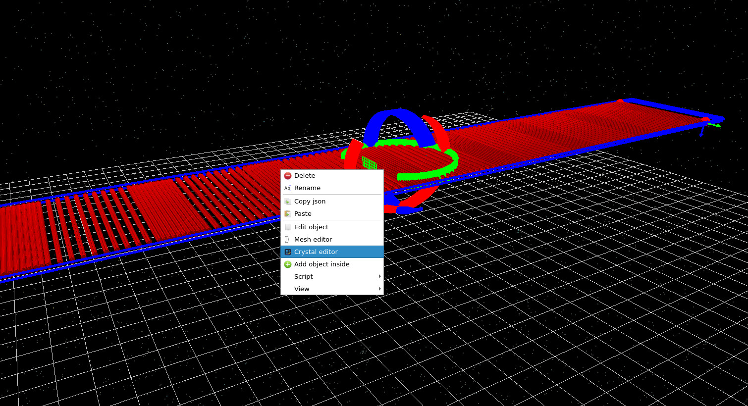
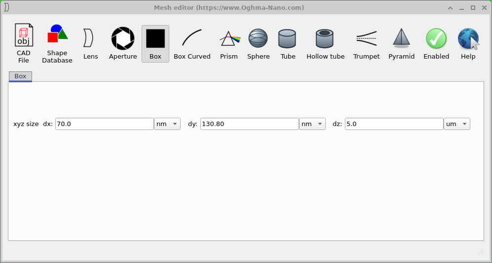
If you right-click on the DFB structure itself, you are given a few options, including the Mesh editor and the Crystal editor (see ??). Clicking on the Mesh editor (see ??) shows the dimensions of the box itself. It should be remembered that the transfer matrix method is a one-dimensional method, so it does not really matter what the other dimensions of the structure are — the only thing that matters is the width along the propagation axis, not necessarily the other dimensions of the box. If you were doing FDTD in two dimensions, the other dimension would be more important.
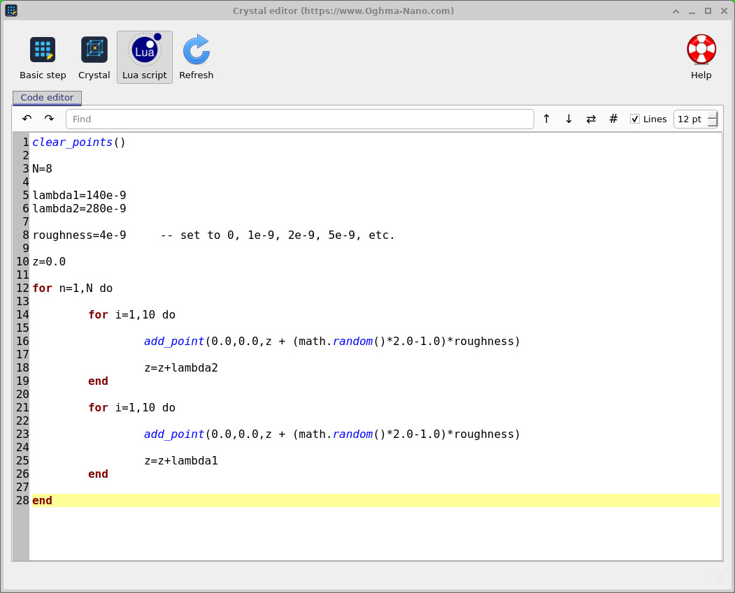
Select the Crystal editor from the same menu
(see ??)
to view the Lua script used to generate the grating structure. Rather than defining each grating element manually,
the complete structure is constructed programmatically. Clicking Refresh reruns the script and
regenerates the geometry. In this example, math.random introduces a small positional variation,
so the grating changes slightly each time it is regenerated. This effect can be seen in
??,
where the grating geometry is updated every two seconds to illustrate the random variation introduced into the period.
clear_points()

N = 200
radius = 1.5e-6
pitch = 3e-6
turns = 6

for i = 1, N do
t = (i / N) * turns * 2 * math.pi

-- first helix strand
x1 = radius * math.cos(t)
y1 = radius * math.sin(t)
z1 = (i / N) * turns * pitch
add_point(x1, y1, z1)

-- second helix strand offset by pi (opposite side)
x2 = radius * math.cos(t + math.pi)
y2 = radius * math.sin(t + math.pi)
add_point(x2, y2, z1)

end 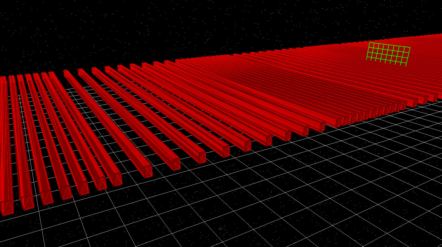
The script begins by clearing any previously generated points, then defines the parameters that control the geometry. The main for loop steps through the structure one position at a time. On each pass, the current value of i is used to calculate the coordinates of the next part of the geometry, and these coordinates are then added to the structure using add_point(). A second set of coordinates is calculated within the same loop to generate the corresponding point on the opposite side. In the DFB grating example, the same idea is used to place each grating element in sequence. By changing the parameters or adding terms such as math.random(), the script can generate different periods, dimensions or controlled variations in the grating.
6. Choosing the illumination direction
A useful feature of OghmaNano is that the transfer matrix calculation is not restricted to a single propagation direction. In many implementations, the calculation is applied only along the layer stack, for example through the device epitaxy. In OghmaNano, the illumination direction can instead be selected explicitly, allowing the same structure to be simulated along any of the principal axes.
To choose the illumination direction, open the Optical ribbon
(see ??)
and select Light Sources to open the light source editor
(see ??).
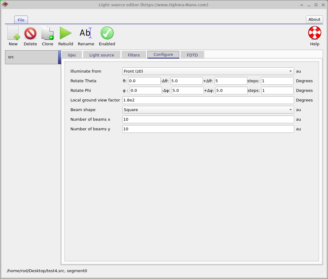
In the Configure tab, use the Illuminate from field to select
x0, x1, y0, y1, z0 or z1.

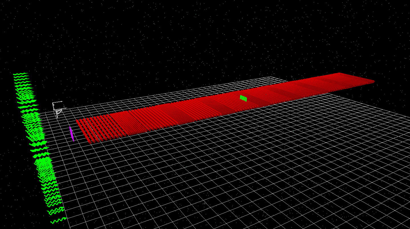
z0, with the light source at one end of the grating.
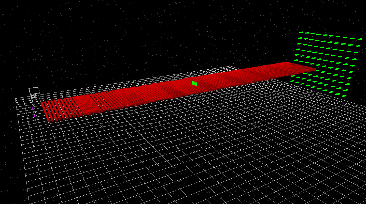
z1, with the light source moved to the opposite end.
In this example, changing the illumination from z0
(see ??)
to z1
(see ??)
simply moves the light source to the opposite side of the grating. For this reciprocal structure the optical response is the same from either direction, but the option is useful when studying asymmetric structures or comparing propagation from opposite sides.
7. Conclusion
In this tutorial, we used OghmaNano to simulate a distributed feedback (DFB) mirror and Bragg grating with the finite-difference transfer matrix method. You learned how to generate a two-period grating using Lua scripting, introduce controlled randomness to represent fabrication tolerances, run the optical calculation, and interpret the resulting reflection, transmission and absorption spectra. You also saw how the illumination direction can be selected along any of the principal axes rather than being restricted to a fixed epitaxial direction. These techniques can be used to study DFB and DBR laser mirrors, fibre Bragg gratings, optical filters, dielectric mirrors and other wavelength-selective photonic structures, as well as more complex gratings containing multiple periods, disorder or custom geometries.