
 ☰
☰
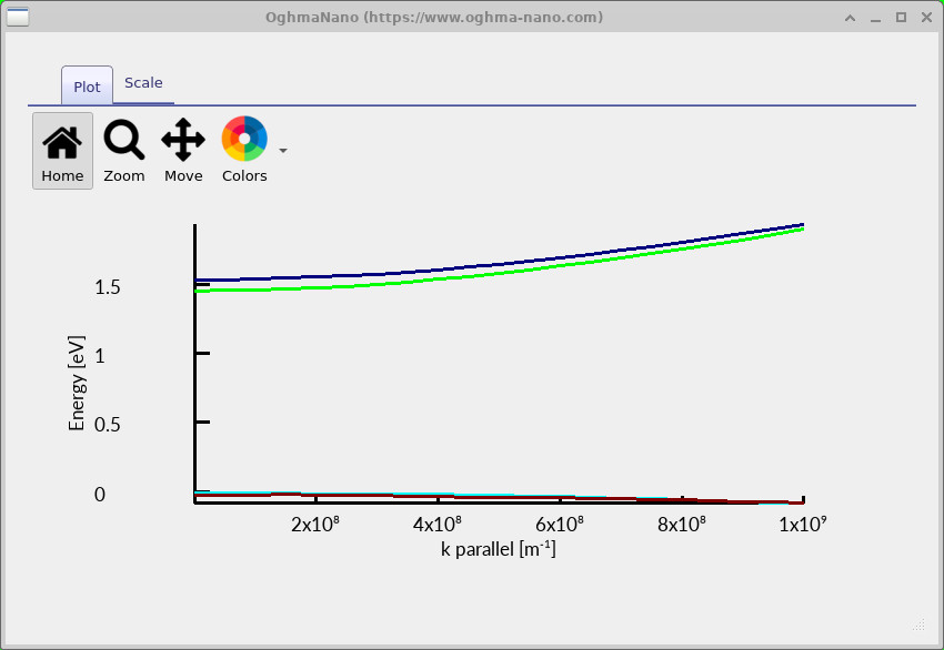
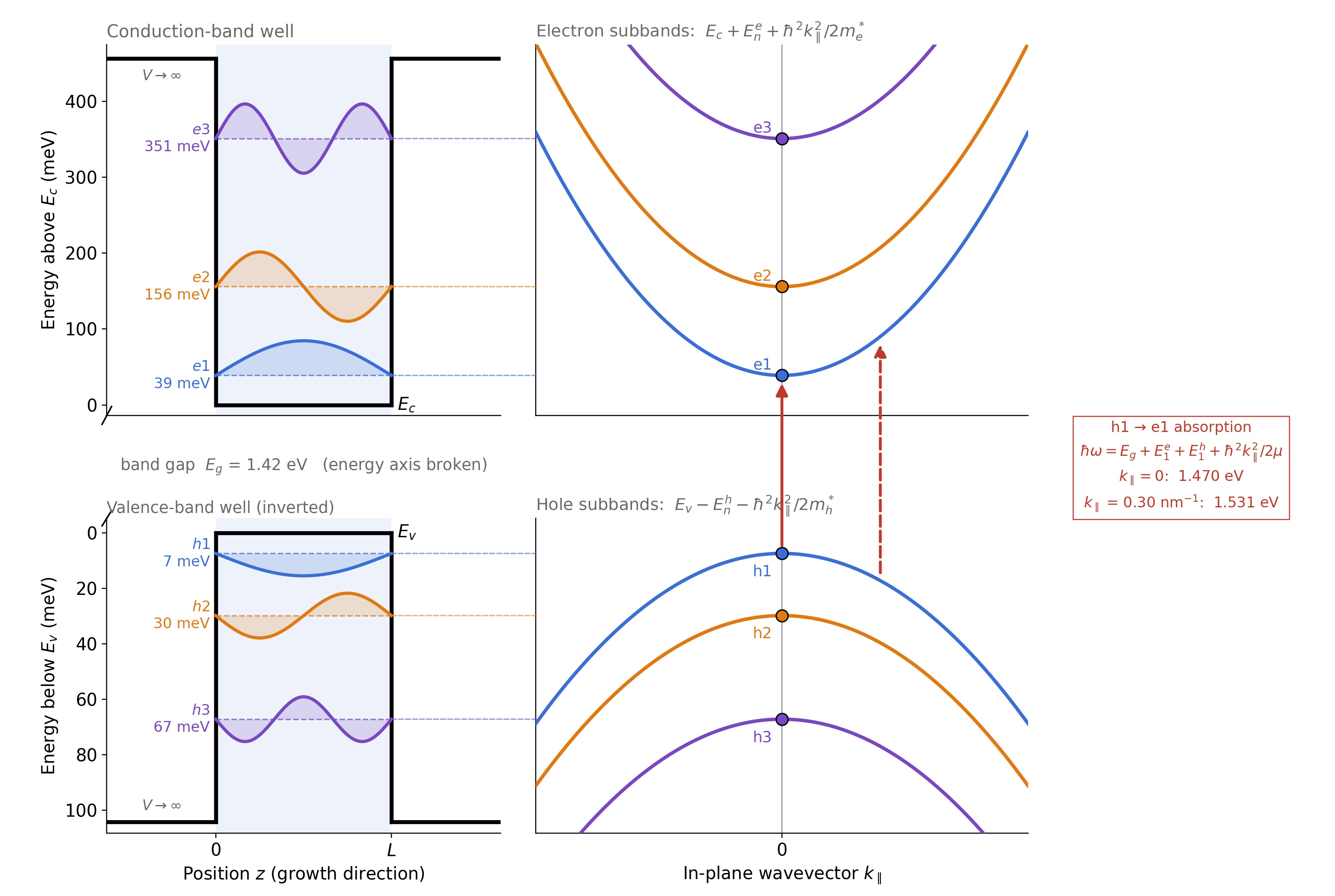

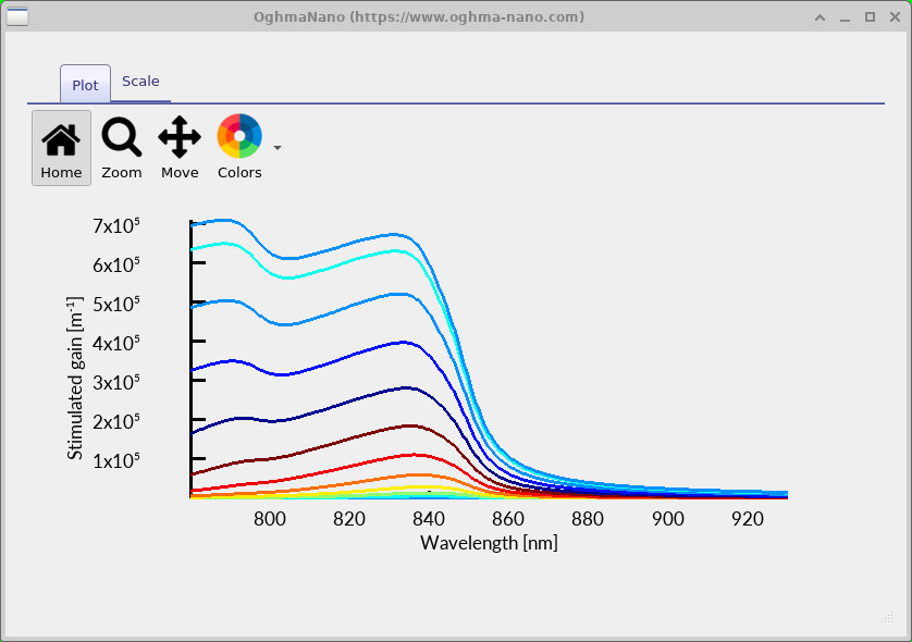
OghmaNano contains a family of semiconductor band-structure, quantum-well and k·p solvers for calculating electronic states in both two-dimensional quantum wells and bulk semiconductors. The models calculate confined electron and hole states, electronic band dispersion, wavefunctions, band mixing and optical matrix elements, and can be coupled to calculations of optical absorption, spontaneous emission, stimulated emission, gain, carrier scattering and mobility.
A range of band-structure models is available for different semiconductor materials and crystal structures:
Together, these models allow OghmaNano to calculate both two-dimensional quantum-well subbands and three-dimensional bulk semiconductor band structures. For quantum wells, carriers are confined along the growth direction while remaining free to move parallel to the layers. In a multiband k·p calculation the growth-direction wavevector is replaced by the envelope-function operator
\[ k_z \longrightarrow -i\frac{d}{dz}, \]
and the resulting coupled equations are solved across the semiconductor heterostructure. Repeating the calculation as a function of in-plane wavevector produces the two-dimensional subband dispersion. Bulk models, such as the perovskite solver, instead solve the Hamiltonian directly as a function of the three-dimensional wavevector \(\mathbf{k}=(k_x,k_y,k_z)\).
The calculated eigenvalues and eigenvectors provide more than a band diagram. They form the starting point for simulations of optical transitions , absorption, spontaneous emission, stimulated emission and optical gain, as well as carrier scattering, relaxation times and mobility where supported. These capabilities make the band-structure solvers applicable to the modelling of semiconductor lasers, LEDs, photodetectors, quantum-well heterostructures, high-mobility semiconductor channels, silicon/SiGe devices and metal-halide perovskite solar-cell and light-emitting materials.
For a general introduction to the underlying physics, see quantum wells and carrier confinement and the introduction to k·p theory .
Calculating the electronic band structure is only the first stage of the simulation. Once the energies and wavefunctions of the electronic states are known, OghmaNano can use them to calculate a range of optical and charge-transport properties. These include optical absorption, spontaneous and stimulated emission, optical gain, phonon scattering rates, carrier relaxation times and charge-carrier mobility.
The same basic idea underlies many of these calculations: a carrier makes a transition from an initial electronic state to a final state, with the transition probability determined by the coupling between the two states. In the weak-interaction limit this is described by Fermi's golden rule,
\[ W_{i\rightarrow f} = \frac{2\pi}{\hbar} \left|\langle f|\hat H_{\mathrm{int}}|i\rangle\right|^2 \delta(E_f-E_i). \]
The interaction Hamiltonian \(\hat H_{\mathrm{int}}\) depends on the physical process being considered. For an optical transition it describes the interaction between the electronic states and the electromagnetic field. For carrier scattering it can instead describe interactions with lattice vibrations, including acoustic phonons or longitudinal optical (LO) phonons. The calculated band structure therefore provides a common electronic basis from which both optical and transport properties can be derived.
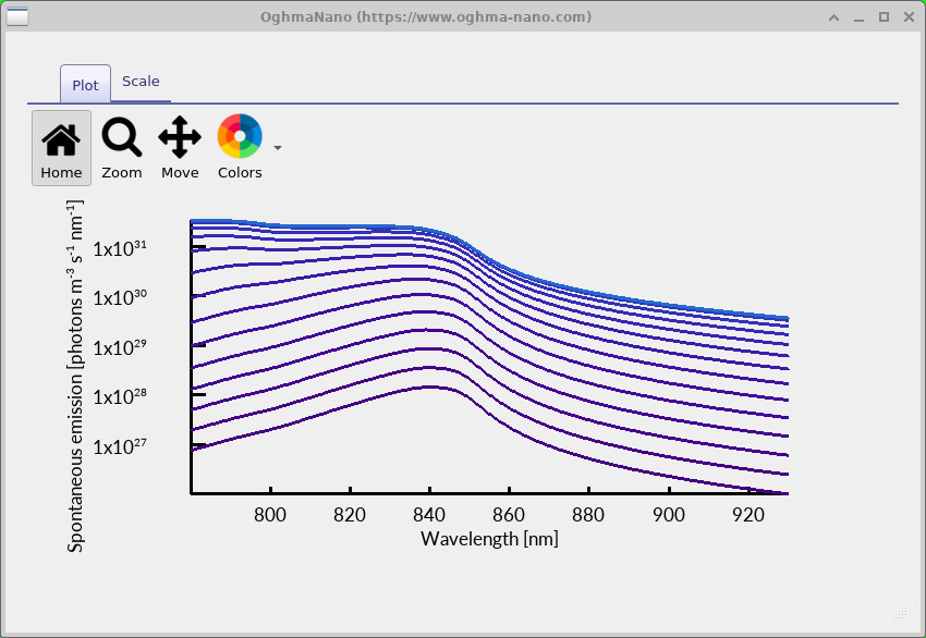
For optical calculations, OghmaNano combines the calculated conduction- and valence-band states with their optical matrix elements and carrier occupations. Transitions between occupied and unoccupied states can then be summed across the calculated band structure to obtain absorption, stimulated emission, net optical gain and spontaneous emission.
Because multiband k·p eigenvectors retain information about the orbital and spin character of each state, the optical calculation can go beyond simply matching energy levels. Band mixing changes the transition matrix elements and therefore the strength of the optical response. In anisotropic systems such as wurtzite semiconductors, this also allows TE- and TM-polarised optical transitions to be treated separately.
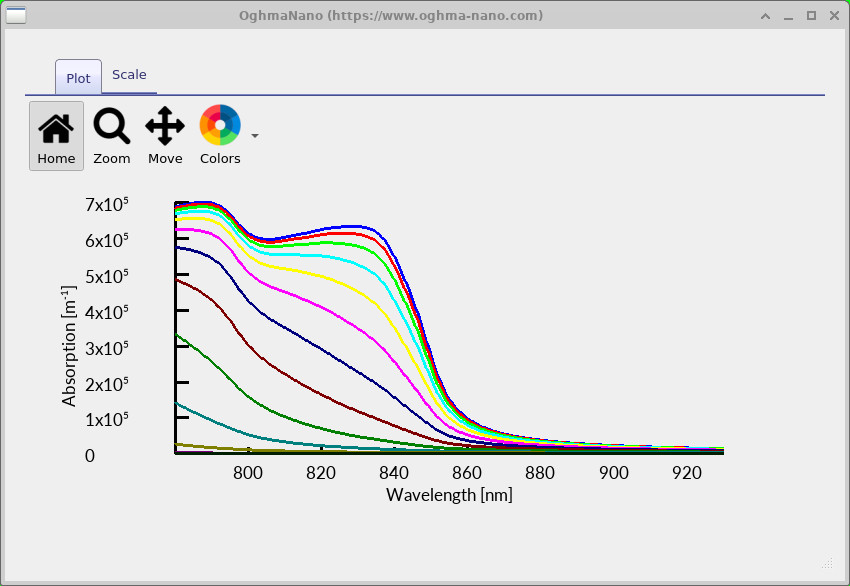
The electronic states can also be used to calculate the probability that a carrier is scattered from one part of the band structure to another. Depending on the material and model, OghmaNano can include mechanisms such as acoustic-phonon scattering and Fröhlich polar-optical-phonon scattering . These processes determine carrier lifetimes, momentum relaxation and ultimately charge-carrier mobility.
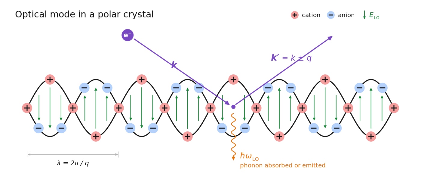
Fröhlich scattering is particularly important in polar semiconductors such as GaAs, InP, GaN and metal-halide perovskites. A longitudinal optical phonon creates an oscillating polarisation field that interacts with an electron or hole. The strength of this interaction is described by the Fröhlich matrix element,
\[ M(q) = -\frac{i}{q} \left[ \frac{e^2\hbar\omega_{LO}}{2V\varepsilon_0} \left( \frac{1}{\varepsilon_\infty} - \frac{1}{\varepsilon_s} \right) \right]^{1/2}. \]
Here \(q\) is the phonon wavevector, \(\omega_{LO}\) is the LO-phonon angular frequency, and \(\varepsilon_\infty\) and \(\varepsilon_s\) describe the electronic and static dielectric screening of the material. The \(1/q\) dependence reflects the long-range nature of the polar interaction.
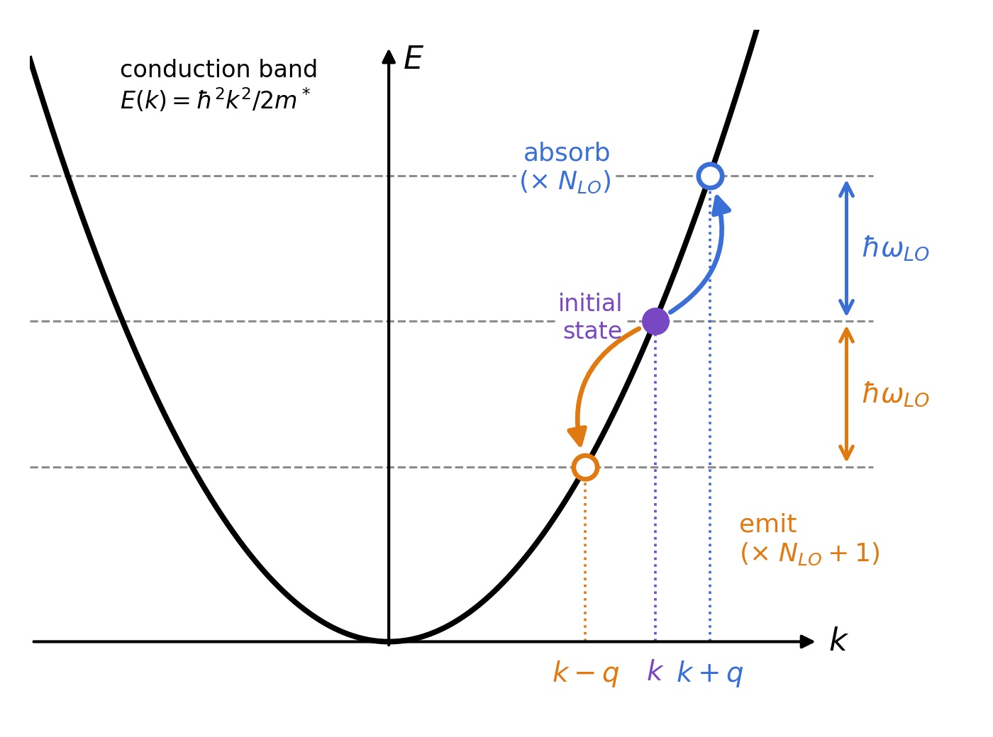
Applying Fermi's golden rule and integrating over the available final states gives the carrier scattering rate. For LO-phonon absorption, for example,
\[ \begin{aligned} \frac{1}{\tau_{\mathrm{abs}}(\mathbf{k})} ={}& \frac{2\pi}{\hbar} \frac{V}{(2\pi)^3} \int d^3q\; \frac{e^2\hbar\omega_{LO}}{2V\varepsilon_0} \left( \frac{1}{\varepsilon_\infty} - \frac{1}{\varepsilon_s} \right) \frac{N_{LO}}{q^2} \\[4pt] &\times \delta\left( E(\mathbf{k}+\mathbf{q})- E(\mathbf{k})- \hbar\omega_{LO} \right). \end{aligned} \]
The Dirac delta function enforces conservation of energy, while the integration over \(\mathbf{q}\) sums over the phonon wavevectors capable of connecting the initial and final electronic states. LO-phonon emission is calculated in the same way, except that the carrier loses an energy \(\hbar\omega_{LO}\). In contrast, acoustic-phonon scattering describes interactions with the lower-energy lattice vibrations associated with elastic deformation of the crystal.
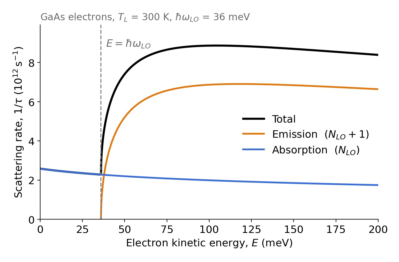
A scattering event does not necessarily destroy all of a carrier's directed momentum. Forward scattering, for example, changes the carrier direction only slightly, while backscattering strongly opposes the electrical current. For transport calculations OghmaNano can therefore use a momentum-relaxation rate rather than simply taking the inverse of the total scattering rate.
Once the transport relaxation time has been calculated across the electronic band structure, the mobility can be obtained by averaging the velocity and scattering properties of the electronic states that participate in transport. Within the relaxation-time approximation,
\[ \mu_{ij} = \frac{e}{n} \sum_b \int \frac{d^3k}{(2\pi)^3} v_{b,i}(\mathbf{k}) v_{b,j}(\mathbf{k}) \tau_{\mathrm{tr},b}(\mathbf{k}) \left( -\frac{\partial f}{\partial E} \right)_{E_b(\mathbf{k})}. \]
The carrier velocity is obtained directly from the calculated electronic dispersion,
\[ \mathbf{v}_b(\mathbf{k}) = \frac{1}{\hbar} \nabla_{\mathbf{k}}E_b(\mathbf{k}). \]
This connects the calculated band structure directly to an experimentally measurable transport quantity. Rather than assuming a single constant effective mass and scattering time, the calculation can account for the way carrier velocity and scattering vary across the electronic bands.
For Si/SiGe quantum wells, OghmaNano can calculate acoustic-phonon scattering and two-dimensional electron or hole mobility using the silicon Δ-valley and Luttinger–Kohn models. For bulk metal-halide perovskites, the calculated eight-band electronic structure can be combined with Fröhlich electron–phonon scattering to obtain carrier relaxation times and phonon-limited mobility.
Worked examples are available in the Si/SiGe electron mobility tutorial , Si/SiGe hole mobility tutorial and perovskite band-structure and mobility tutorial .
The examples supplied with OghmaNano provide ready-made starting points for each band-structure model. For quantum-well optical calculations, the GaAs/AlGaAs eight-band k·p tutorial demonstrates the calculation of electronic subbands, absorption, stimulated emission, optical gain and spontaneous emission.
For bulk calculations, the perovskite band-structure and mobility tutorial shows how to calculate the electronic bands of CsPbX3 and MAPbX3 materials and use the resulting states to calculate Fröhlich scattering and charge-carrier mobility.
Further theoretical background is available in the k·p theory guide , optical-transition theory and Fröhlich scattering theory .
For an introduction to quantum confinement, begin with quantum wells and carrier confinement . The parabolic-band tutorial introduces the simplest quantum-well model, while the k·p theory guide explains how several electronic bands are coupled in a multiband Hamiltonian.
For a practical starting point, try the GaAs/AlGaAs eight-band k·p tutorial or the bulk perovskite band-structure and mobility tutorial .
Explore the quantum and band-structure modelling tools.
Start with the quantum-well introduction, read the k·p theory guide, or run the 8-band GaAs/AlGaAs tutorial.