OghmaNano provides an advanced organic photovoltaic (OPV) simulation framework for modelling solar cells from optical simulation through to full electrical device modelling. The simulator solves the internal device physics directly using a coupled drift-diffusion framework, including explicit, non-equilibrium trap-state dynamics required for disordered semiconductors such as OPVs, allowing direct inspection of how optical absorption, carrier transport, trapping, recombination, energetics, and contacts determine the final JV curve. The same framework applies across bulk heterojunctions, planar and tandem devices, parameter extraction, spectra, transient and frequency-domain analysis, and extends to (perovskite solar cells, silicon-based structures, large-area devices). It combines realistic thin-film optics with full electronic transport, and includes large-area circuit models to study spatial non-uniformities and scaling from cells to modules. Simulations can be compared directly with experiment (JV, PL, EL, TPV, CELIV, impedance spectroscopy, IMPS, IMVS), within a single framework that retains access to the full internal state of the device.
At the heart of the OPV solver is the coupled solution of electrostatics, carrier transport, optical generation, and dynamic trap-state kinetics. Unlike steady-state Shockley–Read–Hall models, trap occupation is treated explicitly as a time-dependent quantity, allowing traps to act as both recombination centres and charge reservoirs that reshape the internal electrostatics. The electrostatic potential is obtained from Poisson’s equation,
$$ \nabla \cdot \left( \varepsilon \nabla \phi \right) = -q \left( p - n + N_D^+ - N_A^- + \rho_{\mathrm{trap}} \right), $$where \(\rho_{\mathrm{trap}}\) represents the charge stored in occupied trap states. In disordered semiconductors such as OPVs, this trapped charge is not a passive recombination pathway: it dynamically modifies the internal electric field and therefore feeds back directly into transport, recombination, and charge extraction. For a fuller discussion, see the need for trap states and non-equilibrium SRH theory.
Electrons and holes are transported through the active region using the drift-diffusion equations,
$$ \mathbf{J}_n = q \mu_n n \mathbf{E} + q D_n \nabla n $$ $$ \mathbf{J}_p = q \mu_p p \mathbf{E} - q D_p \nabla p, $$together with the continuity equations,
$$ \frac{\partial n}{\partial t} = \frac{1}{q}\nabla \cdot \mathbf{J}_n + G - R $$ $$ \frac{\partial p}{\partial t} = -\frac{1}{q}\nabla \cdot \mathbf{J}_p + G - R. $$The carrier densities themselves are determined from the density of states and Fermi-level occupation, not from an idealised crystalline picture. In OPVs and other disordered materials the density of states must include trap tails, so that carrier densities, recombination rates, and mobilities are governed by the evolving trap occupancy. Without this, the relation between quasi-Fermi level and carrier density is incorrect, and the resulting device physics is not captured reliably. This issue is discussed in more detail in the trap-state theory page.
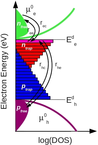
Here the generation term G is supplied by the optical solver, while the recombination term R can include free-to-free recombination, analytical Shockley–Read–Hall recombination, non-equilibrium SRH trapping and recombination, and Auger recombination. In OghmaNano, trap populations evolve dynamically in time through non-equilibrium SRH rate equations, enabling a consistent treatment of steady-state, transient, and frequency-domain experiments within the same framework.
For a given trap level, the occupancy evolves according to a rate equation of the form
$$ \frac{dn_t}{dt} = r_{ec} - r_{ee} - r_{hc} + r_{he}, $$where \(r_{ec}\), \(r_{ee}\), \(r_{hc}\), and \(r_{he}\) are the capture and emission rates for electrons and holes. In real OPV materials this is generalized from a single discrete trap to a broader density of states, so that carrier density, recombination, and transport are governed by the evolving trap landscape rather than by an idealised band-edge picture. This is precisely why non-equilibrium SRH theory and explicit trap-state modelling are central to realistic OPV simulation.
This is one of the main reasons the OPV solver is useful in practice. It does not simply predict a final efficiency number: it allows the user to understand why the efficiency changes. For example, a reduced fill factor might emerge from poor mobility balance, contact barriers, increased recombination, trap filling, or parasitic series resistance, while a reduction in current might originate from weak absorption, optical losses, or inefficient charge extraction. By solving the internal state of the device self-consistently, OghmaNano makes it possible to separate these effects rather than folding them into a single empirical parameter.
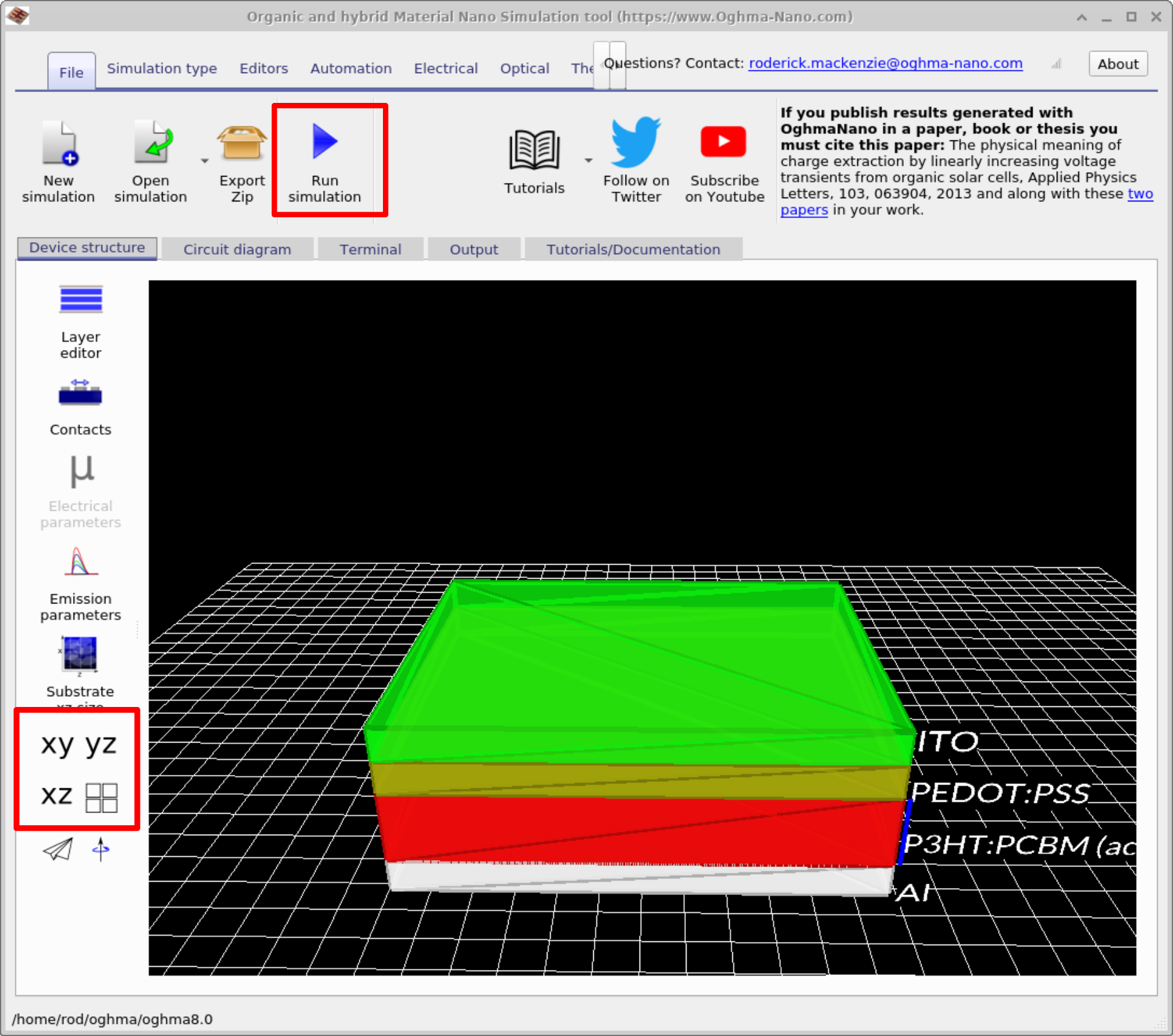
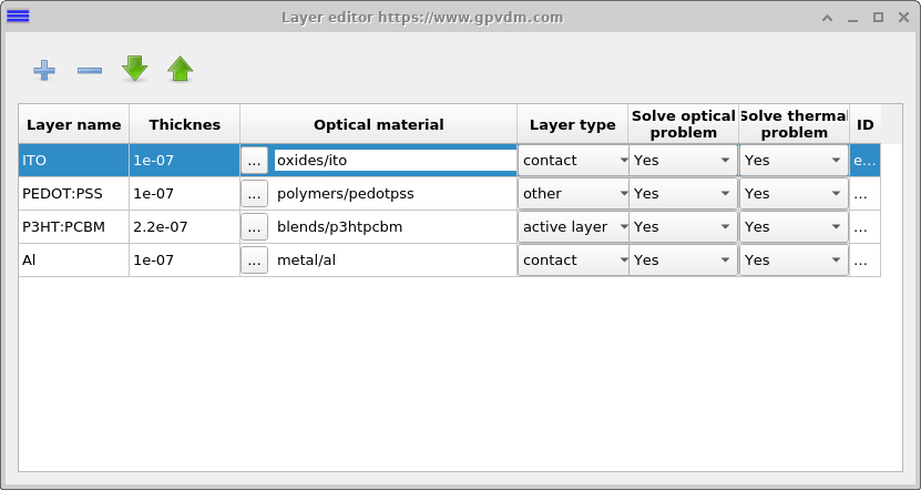
Every OPV simulation depends on three tightly linked components: the layer structure, the optical model, and the electrical and trap-state model. The layer stack is defined in the editor shown in Figure ??, where the user specifies the thickness, optical material, and role of each layer. In a standard device this might include a transparent electrode such as ITO, a hole-transport layer such as PEDOT:PSS, an active layer such as P3HT:PCBM or PM6:Y6, and a metallic back contact. For a practical introduction to editing these structures, see the device-structure tutorial.
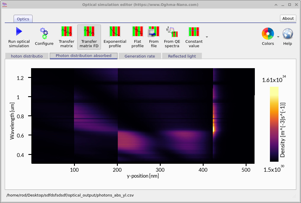
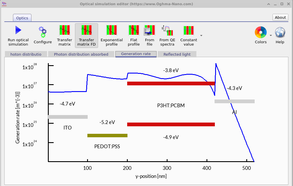
The optics are then solved using thin-film methods such as the transfer-matrix method, which calculates how the electromagnetic field propagates through the multilayer device. This allows the simulator to determine where light of each wavelength is reflected, transmitted, or absorbed. The wavelength-resolved absorption map in Figure ?? shows this directly. From this information the optical solver constructs a generation profile, which is passed to the electrical model as the source term for free-carrier generation.
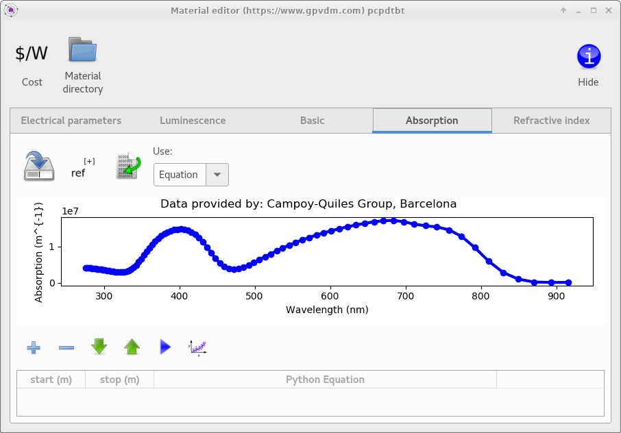
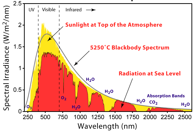
The user can also inspect the optical database and material absorption spectra directly. For example, by comparing the AM1.5G solar spectrum with the absorption coefficient of a polymer such as P3HT, it becomes immediately clear why some material systems generate more current than others: the overlap between the solar spectrum and the absorber’s optical response strongly influences the available photogeneration. That optical generation must then be filtered through the transport physics of a trap-rich active layer before it appears as extracted current.
In disordered organic semiconductors, however, the optical problem is only half the story. The electrically active layer contains a broad distribution of localized states, and these trap states control how injected or photogenerated charge is stored, released, and recombined. This means the relation between applied voltage and carrier density is no longer the simple crystalline-semiconductor picture. Instead, the quasi-Fermi levels move through a trap-filled density of states, and that change in occupancy alters both the effective mobility and the recombination rate. This is why realistic OPV modelling requires an explicit trap-state density of states and a consistent treatment of SRH trapping and recombination.
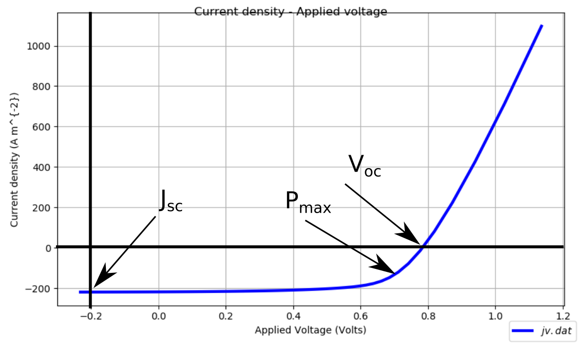
Once the device is solved, the resulting electrical response can be inspected through outputs such as the current-voltage curve shown in Figure ??. From this the user can extract the familiar photovoltaic metrics of short-circuit current density, open-circuit voltage, fill factor, and power conversion efficiency. At the same time, the software can expose much more than a single curve: carrier densities, quasi-Fermi levels, recombination maps, field distributions, trapped charge, spectra, and voltage-dependent sweeps can all be examined. The main interface shown in Figure ?? provides direct access to these workflows, and the quick-start OPV tutorial shows how to begin from a working example.
The OPV solver can be used for a broad range of photovoltaic problems. In research it can model classical P3HT:PCBM cells, modern non-fullerene systems such as PM6:Y6, tandem OPVs, thickness optimisation, contact-limited behaviour, recombination-limited devices, and transient or frequency-domain experiments. In teaching it can be used to introduce the relationship between layer thickness, optical absorption, and JV response. More broadly, it can be used wherever the goal is to connect measured device behaviour to physically meaningful internal parameters.
Because the simulator resolves both optics and electronics, it is especially useful when the user wants to understand not only what the final efficiency is, but how the device arrives there. That includes understanding why a particular active-layer thickness is optimal, why a change in mobility shifts the fill factor, why a contact barrier creates an S-shaped JV curve, why one absorber produces stronger generation than another, or how trap filling changes the voltage dependence of recombination. These themes are explored in the layer and active-layer tutorial, the trap-state theory section, and the non-equilibrium SRH section.
The OPV framework is also a useful bridge between idealised device physics and more practical engineering questions. Small-area cells, calibrated literature examples, transient experiments, impedance spectroscopy, intensity-modulated photocurrent spectroscopy, intensity-modulated photovoltage spectroscopy, and even large-area upscaled devices can be studied within the same wider OghmaNano environment. This makes the OPV module valuable not only for academic modelling, but also for device prototyping, training, and virtual design before fabrication.
OghmaNano includes a growing set of example OPV simulations and step-by-step tutorials. These are a good way to move quickly from the underlying method to practical device analysis. The examples cover both introductory organic solar-cell problems and more detailed studies of optics, layer structure, contacts, parameter variation, and dynamic measurements.
Useful starting points include the quick-start OPV tutorial, the OPV optics and light tutorial, the device-structure and layer tutorial, the impedance spectroscopy tutorial, the IMPS tutorial, the IMVS tutorial, and the large-area PM6:Y6 solar-cell tutorial. For the underlying theory, see the sections on drift-diffusion theory, electrostatics, the drift-diffusion equations, charge-carrier density, free-to-free recombination, non-equilibrium SRH trapping and recombination, analytical SRH recombination, Auger recombination, and the need for trap states. Taken together, these examples show how the same framework can be used for thin-film optics, electrical transport, trap-state kinetics, steady-state JV analysis, transient response, and frequency-domain characterisation.
Try an OPV example.
Start with the quick-start OPV tutorial for a first simulation, then move on to optics and absorption, device structure and active layers, impedance spectroscopy, IMPS, IMVS, or large-area PM6:Y6 simulations.
For the physics behind disordered-semiconductor modelling, see why trap states are required, how non-equilibrium SRH trapping and recombination are treated, and the analytical SRH limit.