Modelling Distributed Trap States in Disordered Semiconductors
The tutorial is written as a general introduction to trap-state modelling in disordered semiconductors. PM6:Y6 is used as the worked example because it is a well-known organic photovoltaic material, but the same modelling ideas apply more broadly to organic semiconductors, amorphous silicon, oxide semiconductors, perovskites and other thin-film materials where localized states form a distributed density of states inside the bandgap.
1. Introduction: why trap distributions matter in disordered semiconductors
Trap states are central to the behaviour of many disordered semiconductors, including organic semiconductors, amorphous silicon, oxide semiconductors, perovskites and other thin-film photovoltaic materials. The difference between ordered and disordered semiconductors can be seen in ??. In highly ordered semiconductors such as extremely high-purity crystalline silicon, often described as six-nines or nine-nines pure material, there are relatively few trap states within the bandgap. These isolated trap states are illustrated by region a in ??. In such systems, recombination through these defects can often be described using the standard Shockley–Read–Hall (SRH) recombination equation:
\[ R_{SRH}=\frac{np-n_i^2} {\tau_p(n+n_1)+\tau_n(p+p_1)} \]
For the step-by-step mathematical derivation, see the Shockley–Read–Hall recombination derivation.
This equation assumes that recombination occurs through a single discrete mid-gap trap state, which is often an appropriate approximation for relatively ordered semiconductors/devices such as silicon p–n diodes and gallium-arsenide p–n diodes. However, as the degree of disorder increases, it becomes less useful to think of traps as isolated defects and more useful to describe them as an entire distribution of states within the bandgap. This distribution of states is commonly referred to as the density of trap states or density of states (DOS). The right-hand side of ?? illustrates this situation for a disordered semiconductor such as an organic semiconductor or amorphous silicon. Region b represents a distribution of electron-containing trap states close to the conduction band, region d represents a distribution of hole-containing trap states close to the valence band, and region c represents a distribution of deeper mid-gap states.
In ordered semiconductors, the standard Shockley–Read–Hall (SRH) expression is often sufficient because trap states are usually sparse and can often be approximated as isolated defect levels. In disordered semiconductors this approximation breaks down: the material contains a broad distribution of localized states extending through the band gap, so assuming traps are a single point defect is insufficient. A single-level SRH expression treats the trap as one discrete energy level, so it cannot describe how carriers populate a broad distribution of localized states. In a disordered semiconductor, this occupation determines the balance between mobile and trapped charge, and therefore fixes the relation between total carrier density and quasi-Fermi-level position. If that relation is wrong, the model also gives the wrong recombination rate, effective mobility and J–V behaviour. To model disordered devices correctly, the occupation of the trap distribution must be solved explicitly using trapping, detrapping and recombination rate equations coupled self-consistently to the drift–diffusion and Poisson equations. The resulting trapped population is not a small correction: it can dominate charge storage, transport, recombination, mobility, dark current, open-circuit voltage and the shape of the photovoltaic JV curve.
2. Shockley–Read–Hall trapping and detrapping in disordered semiconductors
Many readers first encounter Shockley–Read–Hall (SRH) recombination through the compact steady-state recombination equation given above. However, this compact equation is only a simplified result derived from the broader SRH rate-equation formalism; the mathematical steps are given in the Shockley–Read–Hall recombination derivation. At its core, SRH theory describes the filling and emptying of a trap state through carrier capture and escape processes, as illustrated in ??. Electrons may be captured into the trap and later thermally emitted back into the conduction band, while holes may also be captured and emitted. When both an electron and a hole occupy the same trap state, recombination occurs.
The underlying SRH formalism is therefore fundamentally a rate-equation model describing carrier trapping, detrapping and recombination:
\[ \frac{dn_t}{dt}=r_{ec}-r_{ee}-r_{hc}+r_{he} \]
Here, \(r_{ec}\) is the electron capture rate into the trap, \(r_{ee}\) is the electron escape rate back into the conduction band, \(r_{hc}\) is the hole capture rate, and \(r_{he}\) is the hole escape rate. One of the key physical ideas behind SRH theory is that the escape rates (\(r_{ee}\) and \(r_{he}\)) depend strongly on the energetic depth of the trap, whereas the capture rates (\(r_{ec}\) and \(r_{hc}\)) depend mainly on whether the trap is occupied. Shallow traps therefore release carriers relatively easily, while deep traps can store charge for long periods of time.
OghmaNano solves the full SRH trapping formalism rather than making the simplifying assumptions normally used to derive the compact steady-state SRH recombination equation. In practice, this means that a separate trapping equation is solved for each trap level within the density of states. This enables the simulator to model trapped charge, trap filling, trap-assisted recombination, electrostatic band bending, and distributed trap populations in highly disordered semiconductors such as organic semiconductors and amorphous silicon.
In this tutorial, we will explore how distributed trap states are implemented and solved in OghmaNano, and how trapping, detrapping and trapped charge influence the behaviour of disordered semiconductor devices.
3. Worked example: creating a PM6:Y6 disordered semiconductor simulation
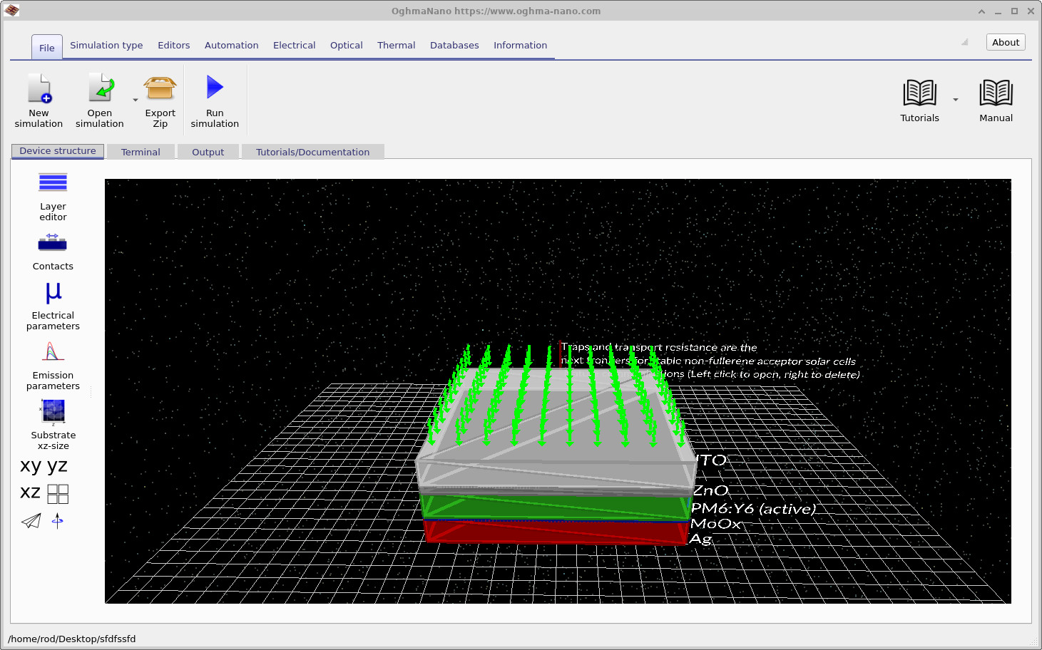
Start OghmaNano and click New simulation. This opens the library of available device types, shown in ??. Double-click the Organic solar cells icon to open the OPV example library. From the list of available PM6:Y6 examples, choose PM6:Y6_E10_0hrs, shown in ??. A generic drift-diffusion simulation could also be used for this tutorial; however, this PM6:Y6 example has already been configured with a trap-state distribution and band structure that match the results shown here. When prompted, save the simulation to a folder where you have write access.
💡 Tip: For best performance save to a local drive such as
C:\. Simulations stored on network, USB, or cloud folders
(e.g. OneDrive) can run slowly due to heavy read/writes.
After the simulation has been created, the main OghmaNano window opens, as shown in ??. The PM6:Y6 device is shown as a layered solar-cell stack. The active layer is the disordered semiconductor region in which the distributed trap states will be modified.
4. Setting the simulation to run in the dark
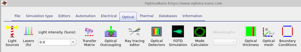
Before starting the simulation, we first need to configure the device to run in the dark. Open the optical ribbon shown in ?? and set the light intensity to 0.0 Suns. This ensures that the generated JV curves correspond to dark JV measurements rather than illuminated photovoltaic operation. Dark simulations are often particularly useful when studying trap states because they reveal carrier injection, trap filling, recombination and electrostatic effects much more clearly than illuminated simulations, where photocurrent can mask many of these processes.
5. Defining the trap density of states
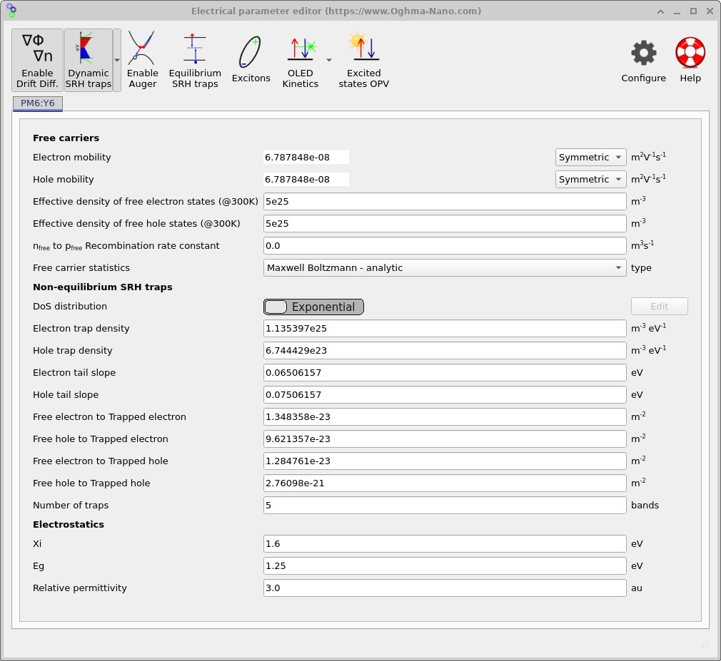
From the main window, open the Electrical parameters editor for the PM6:Y6 active layer using the device-structure tab. This will open the editor shown in ??. When the Dynamic SRH traps option is enabled, OghmaNano solves a distribution of trap states in energy space which resembles the distribution illustrated in ??.
By default, the trap distribution is assumed to follow an exponential density of states. For the LUMO-side tail the density of states is written as
\[ \rho_\mathrm{LUMO}(E)=N_{t,n}\exp\left(\frac{E-E_C}{E_{U,n}}\right), \]
while for the HOMO-side tail it is written as
\[ \rho_\mathrm{HOMO}(E)=N_{t,p}\exp\left(\frac{E_V-E}{E_{U,p}}\right). \]
Here \(N_{t,n}\) and \(N_{t,p}\) are the electron and hole trap-density prefactors, while \(E_{U,n}\) and \(E_{U,p}\) are the corresponding Urbach tail energies. Within the user interface shown in ??, these correspond respectively to the parameters Electron trap density, Hole trap density, Electron tail slope and Hole tail slope in the Non-equilibrium SRH traps section of the electrical parameter editor.
The editor also contains the capture cross sections controlling the rates of the SRH trapping processes discussed earlier. The parameters Free electron to Trapped electron and Free hole to Trapped electron govern the electron capture and hole capture processes (\(r_{ec}\) and \(r_{hc}\)), while Free electron to Trapped hole and Free hole to Trapped hole govern the corresponding escape processes (\(r_{ee}\) and \(r_{he}\)). Together, these parameters determine how rapidly carriers are captured into and emitted from the trap distribution.
Finally, the Number of traps parameter controls the number of discretised trap levels used to approximate the analytical density of states. These correspond to the horizontal red and blue trap levels shown in ??. The analytical density of states itself is still defined by the functions \(\rho_\mathrm{LUMO}(E)\) and \(\rho_\mathrm{HOMO}(E)\), while the number of traps determines how finely the distribution is discretised numerically.
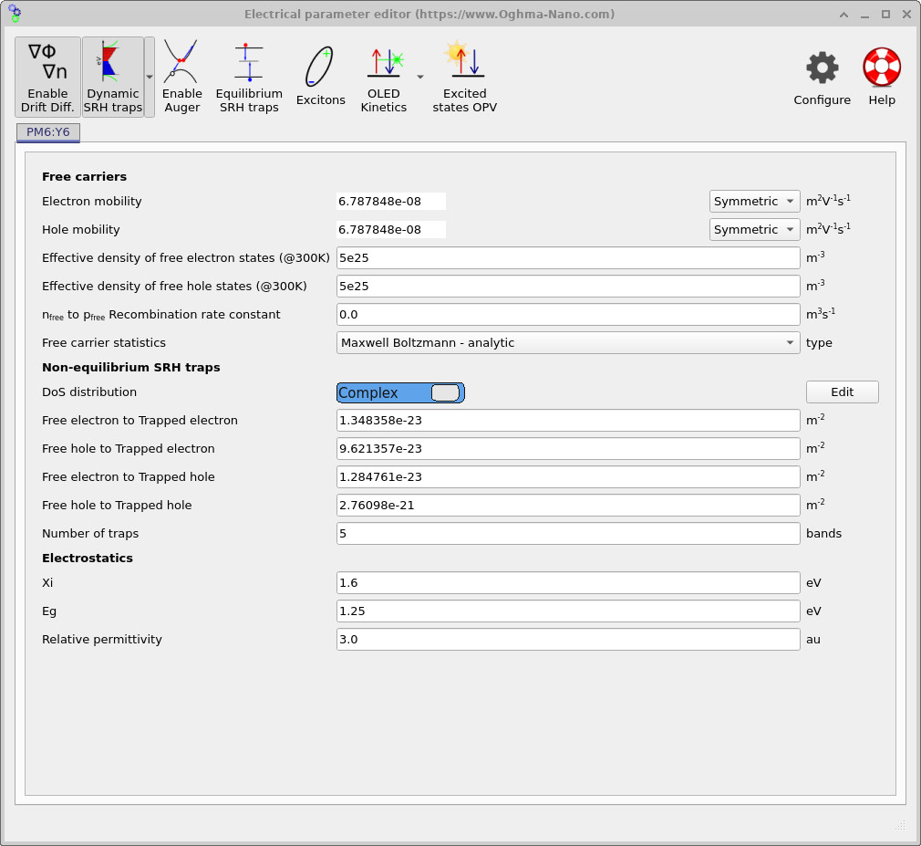
If the simulation is run in this configuration, OghmaNano will assume an exponential density of states corresponding to the equations above. However, OghmaNano also allows much greater control over the exact trap-state distribution. If the Exponential selector is clicked, the mode switches to Complex, as shown in ??. This enables arbitrary mathematical density-of-states shapes to be defined. The complex DOS editor itself can then be opened by clicking the Edit button which appears on the right-hand side of the editor.
6. Define a shallow exponential trap distribution

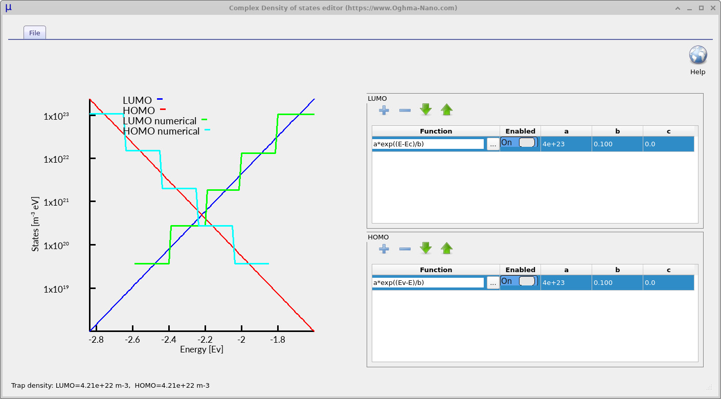
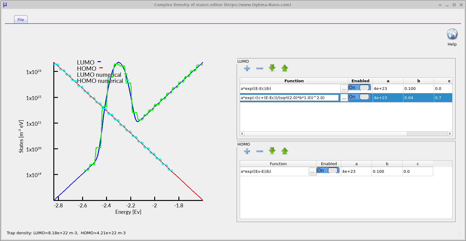
Click Edit to open the complex density-of-states editor. The editor is shown in ??. The upper table defines the LUMO-side trap distribution and the lower table defines the HOMO-side trap distribution. Each row contains a mathematical function, an enable switch and three numerical parameters labelled a, b and c. The plot on the left-hand side of the editor shows the resulting density of states generated from the mathematical functions entered into the tables. The blue analytical curve represents the LUMO-side or conduction-band (\(E_C\)) trap distribution, while the red analytical curve represents the HOMO-side or valence-band (\(E_V\)) trap distribution. These smooth curves correspond to the exact analytical density of states defined by the equations entered into the editor.
The cyan and green staircase curves represent the discretised trap levels actually used internally by the simulator. These staircase levels correspond directly to the Number of traps parameter defined earlier in the electrical parameter editor. Increasing the number of trap levels produces a finer approximation to the analytical density of states and therefore improves the numerical accuracy of the simulation. In practice, simulations using around five trap levels generally produce very good results for many steady-state device simulations. However, simulations involving long transient timescales, such as time-of-flight calculations, can require larger numbers of trap levels, sometimes up to around twenty. Since trap states are solved at every mesh point within the device, increasing the number of trap levels also increases the total mathematical size of the simulation very rapidly, so in practice values much larger than twenty are rarely required.
| Symbol | Meaning in the DOS expression |
|---|---|
| E | Energy coordinate at which the density of states is evaluated |
| EC | Conduction-band edge / LUMO transport level |
| EV | Valence-band edge / HOMO transport level |
| a | A user defined constant |
| b | A user defined constant |
| c | A user defined constant |
In principle, any equation can be entered into the equation editor using the parameters in the table above, and this can be used to construct the density of states.
7. Effect of trap-tail width on dark JV curves and charge density
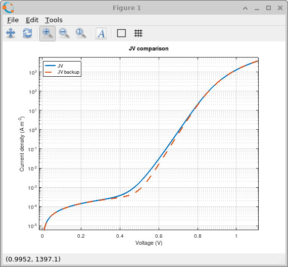
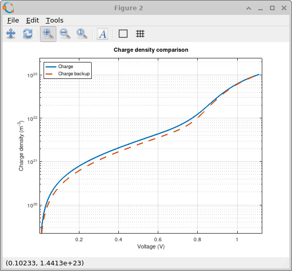
We will now run two simulations and compare the effect of changing the energetic width of the trap distribution. In the complex density-of-states editor, make sure the parameter b is set to 0.025 eV for both the LUMO and HOMO distributions, as shown in ??. This defines the shallow-tail case, where the density of trap states decays relatively quickly away from the band edges and therefore only a limited number of deep trap states are present within the bandgap.
Running and making a backup copy of the simulation for later:
Return to the main window and run the simulation by clicking the blue Run simulation button or by pressing F9.
When the calculation has finished, open the simulation directory using Windows Explorer.
The file jv.csv contains the dark JV curve, while charge.csv contains the total charge stored within the device as a function of voltage.
Make backup copies of these files using Windows Explorer, and rename the copied files to jv.bak and charge.bak.
These backup files will store the shallow-tail simulation results so they can later be compared against the broader trap distribution.
Next, reopen the complex DOS editor and increase the parameter b to 0.100 eV for both the LUMO and HOMO distributions, as shown in
??.
This broadens the trap distribution so that trap states extend further into the bandgap.
Run the simulation again.
After the second run, the simulation directory should now contain both the original backup files (jv.bak and charge.bak) together with the newly generated output files (jv.csv and charge.csv).
☑ After completing this stage, the simulation directory should contain four files:
jv.csv— the dark JV data for the broad-tail simulation.jv.bak— the dark JV data for the shallow-tail simulation.charge.csv— the charge-density data for the broad-tail simulation.charge.bak— the charge-density data for the shallow-tail simulation.
After running both simulations, you can use Microsoft Excel or the MATLAB and Python scripts below to plot the graphs shown in
??
and
??.
In these comparisons, the .bak files correspond to the shallow-tail simulation, while the new .csv files correspond to the broader-tail simulation.
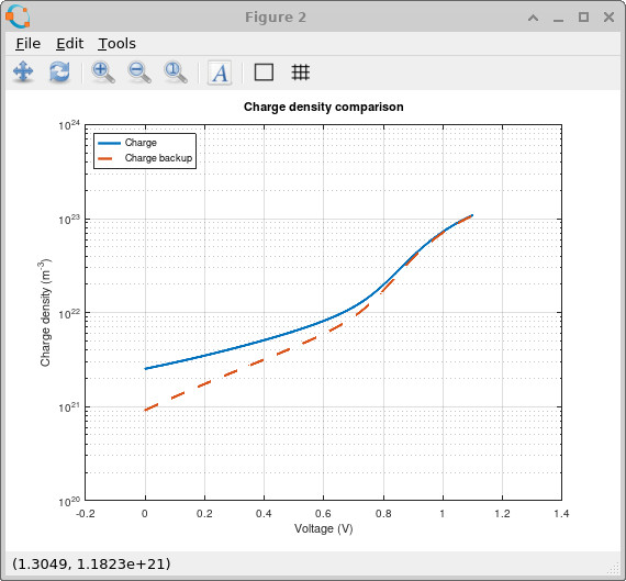
Increasing the Urbach tail energy broadens the density of trap states so that a much larger population of traps extends deep into the bandgap. This directly changes both the recombination current and the amount of trapped charge stored within the device. In the dark JV comparison shown in ??, the broader trap distribution increases the current in the mid-voltage region because carriers can access a much larger population of energetically distributed trap states which participate in trap-assisted recombination and transport.
The effect is also clearly visible in the charge-density comparison shown in ??. The broader trap distribution stores more charge throughout the device because there are now many more energetically accessible states available for carrier occupation. This trapped charge acts as space charge inside the device and therefore changes the electrostatic potential and band bending.
Physically, this is the key difference between modelling a single SRH recombination centre and modelling a full distributed density of trap states. In a disordered semiconductor, the traps are not isolated defects. They form an entire energetic landscape which controls carrier trapping, detrapping, recombination, charge storage and transport simultaneously. This is why trap states must be included in disordered semiconductor device models.
MATLAB / Octave version
clear;
close all;
clc;

% ============================================
% Settings
% ============================================

log_jv = true;
Show full MATLAB script
clear;
close all;
clc;

% ============================================
% Settings
% ============================================

log_jv = true;    % true = semilogy
                  % false = linear plot

% ============================================
% Load data
% ============================================

jv         = load('jv.csv');
jv_bak     = load('jv.bak');

charge     = load('charge.csv');
charge_bak = load('charge.bak');

% ============================================
% Figure 1 : JV
% ============================================

figure;

if log_jv == true

    semilogy(jv(:,1), abs(jv(:,2)), ...
        'LineWidth', 2);

    hold on;

    semilogy(jv_bak(:,1), abs(jv_bak(:,2)), '--', ...
        'LineWidth', 2);

else

    plot(jv(:,1), jv(:,2), ...
        'LineWidth', 2);

    hold on;

    plot(jv_bak(:,1), jv_bak(:,2), '--', ...
        'LineWidth', 2);

end

grid on;
box on;

xlabel('Voltage (V)');
ylabel('Current density (A m^{-2})');

title('JV comparison');

legend( ...
    'JV', ...
    'JV backup', ...
    'Location', 'northwest' ...
);

% ============================================
% Figure 2 : Charge density
% ============================================

figure;

semilogy(charge(:,1), abs(charge(:,2)), ...
    'LineWidth', 2);

hold on;

semilogy(charge_bak(:,1), abs(charge_bak(:,2)), '--', ...
    'LineWidth', 2);

grid on;
box on;

xlabel('Voltage (V)');
ylabel('Charge density (m^{-3})');

title('Charge density comparison');

legend( ...
    'Charge', ...
    'Charge backup', ...
    'Location', 'northwest' ...
);
Python version
import numpy as np
import matplotlib.pyplot as plt

# ============================================
# Settings
# ============================================

log_jv = True
Show full Python script
import numpy as np
import matplotlib.pyplot as plt

# ============================================
# Settings
# ============================================

log_jv = True    # True = semilogy
                 # False = linear plot

# ============================================
# Load data
# ============================================

jv = np.loadtxt("jv.csv")
jv_bak = np.loadtxt("jv.bak")

charge = np.loadtxt("charge.csv")
charge_bak = np.loadtxt("charge.bak")

# ============================================
# Figure 1 : JV
# ============================================

plt.figure()

if log_jv:
    plt.semilogy(jv[:, 0], np.abs(jv[:, 1]), linewidth=2)
    plt.semilogy(jv_bak[:, 0], np.abs(jv_bak[:, 1]), "--", linewidth=2)
else:
    plt.plot(jv[:, 0], jv[:, 1], linewidth=2)
    plt.plot(jv_bak[:, 0], jv_bak[:, 1], "--", linewidth=2)

plt.grid(True)

plt.xlabel("Voltage (V)")
plt.ylabel("Current density (A m$^{-2}$)")
plt.title("JV comparison")
plt.legend(["JV", "JV backup"], loc="upper left")

# ============================================
# Figure 2 : Charge density
# ============================================

plt.figure()

plt.semilogy(charge[:, 0], np.abs(charge[:, 1]), linewidth=2)
plt.semilogy(charge_bak[:, 0], np.abs(charge_bak[:, 1]), "--", linewidth=2)

plt.grid(True)

plt.xlabel("Voltage (V)")
plt.ylabel("Charge density (m$^{-3}$)")
plt.title("Charge density comparison")
plt.legend(["Charge", "Charge backup"], loc="upper left")

plt.show()
8. Effect of trap-tail width under one-sun illumination
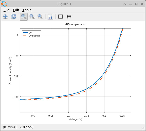
The previous section compared the shallow and broad trap-tail distributions in the dark.
We will now repeat the same comparison under one-sun illumination.
Go to the optical ribbon and set the light intensity back to 1.0 sun.
Then return to the complex DOS editor and set the Urbach tail parameter to b = 0.025 eV for both the LUMO and HOMO distributions.
Run the simulation, then make backup copies of jv.csv and charge.csv using Windows Explorer, renaming them to jv.bak and charge.bak.
Next, return to the complex DOS editor and broaden both trap tails by setting b = 0.100 eV.
Run the simulation again.
The simulation directory should now contain jv.csv, jv.bak, charge.csv and charge.bak.
In this case, the .bak files contain the shallow-tail one-sun simulation, while the new .csv files contain the broad-tail one-sun simulation.
☑ After completing this stage, the simulation directory should contain four files:
jv.csv, jv.bak, charge.csv and charge.bak.
The .bak files contain the shallow-tail illuminated simulation, while the .csv files contain the broad-tail illuminated simulation.
The same MATLAB or Python plotting scripts used above can now be reused without modification.
They will plot jv.csv against jv.bak, and charge.csv against charge.bak.
The resulting illuminated JV comparison is shown in
??,
and the illuminated charge-density comparison is shown in
??.
Under illumination, the trap distribution directly changes the balance between photogeneration, extraction and recombination. A broader tail places more trap states deeper inside the bandgap, increasing the amount of trapped charge and changing the internal electrostatic profile of the device. This modifies the illuminated JV curve because the recombination current and the quasi-Fermi-level splitting are altered by the trapped charge population.
The charge-density plot shows the same physics from a different angle. The broad-tail simulation stores charge differently because carriers are now distributed over a wider range of trap energies. This is why trap distributions matter in photovoltaic simulations: they control not only how much charge is stored, but also where that charge sits energetically and how strongly it reshapes transport, recombination and voltage formation.
9. Visualising trap occupation in energy and position
trap_map directory will be written to the output folder.
Having seen that the trap-state distribution changes the JV and charge-density curves, the next step is to inspect the trap occupation directly.
Open the simulation output directory and look for the trap_map directory.
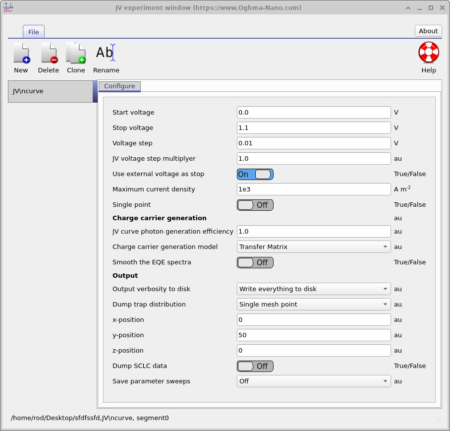
If this directory is not visible, open the Electrical ribbon and click the JV editor.
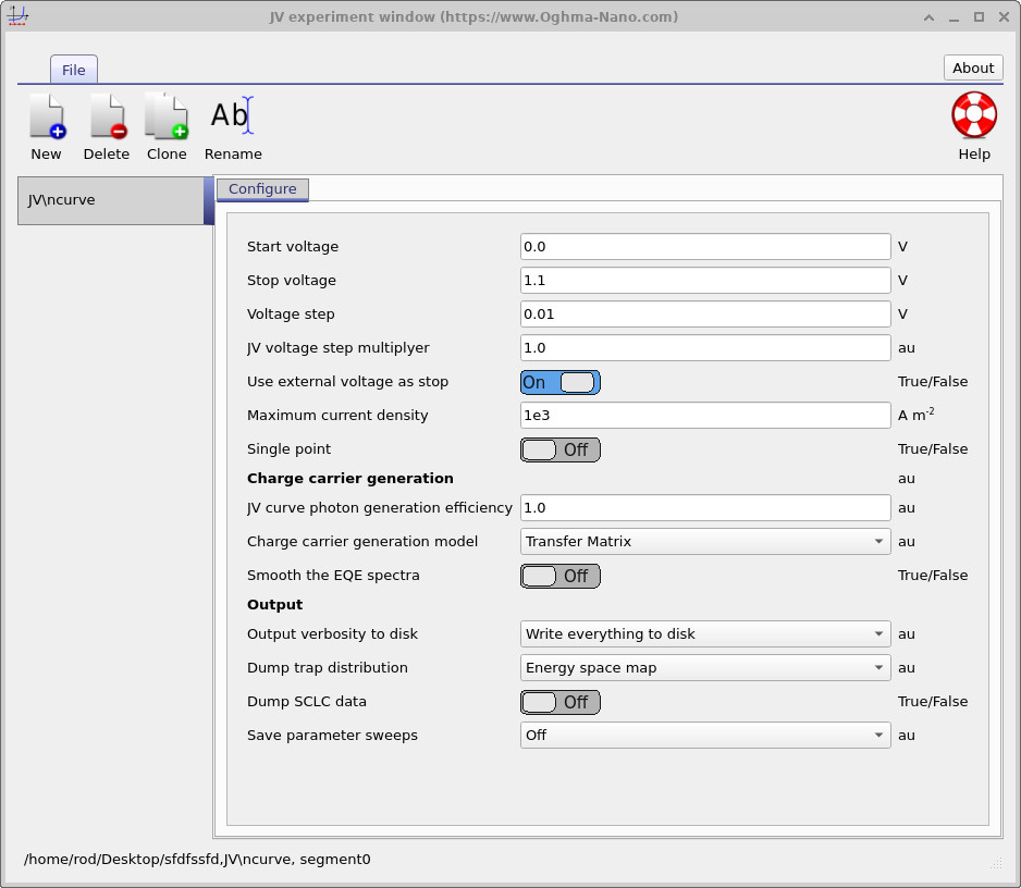
This opens the JV experiment window shown in
??.
In the Output section of the JV editor, set Output verbosity to disk to Write everything to disk.
Then set Dump trap distribution to Energy space map.
Rerun the simulation.
A directory called trap_map should now appear in the output folder.
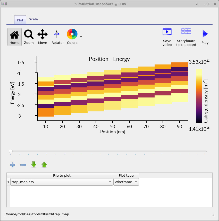
Opening the files in this directory gives an energy-position map of the occupied trap density, as shown in
??.
This map shows the occupation of the distributed trap states as a function of both position and energy. At each voltage point in the JV scan, OghmaNano writes the occupied trap distribution to disk. By moving through the voltage slider, you can see how the trap population fills as the device moves from low voltage towards forward bias.
10. Increase the trap-map resolution
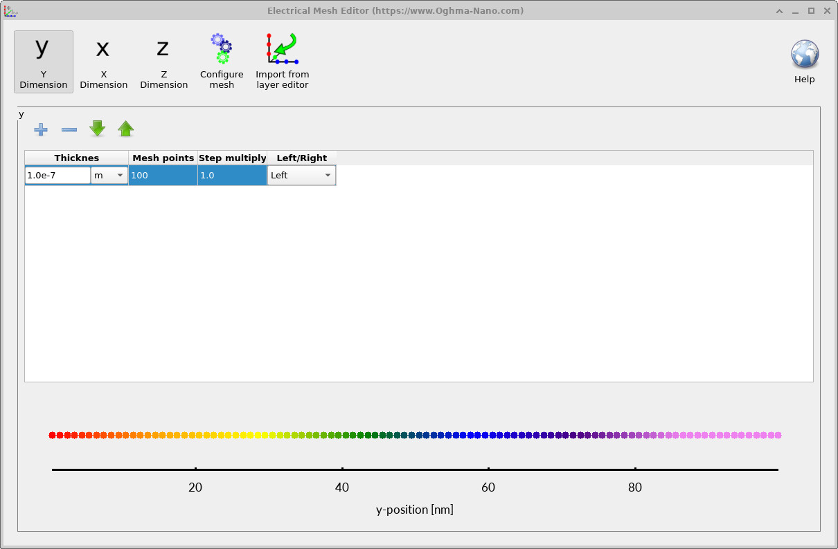
The first trap map is useful for simulation, but the resolution is deliberately low because the default model uses only five trap bands and a modest number of mesh points. For clearer visualisation, return to the electrical parameter editor and increase the Number of traps from 5 to 10 or 20. Then open the mesh editor from the electrical ribbon and increase the number of mesh points in the active-layer direction to around 100, as shown in ??.
Rerun the simulation with the higher-resolution mesh and trap discretisation. The resulting trap maps should look similar to ??, ?? and ??. These plots show how the occupied trap density evolves with applied voltage.
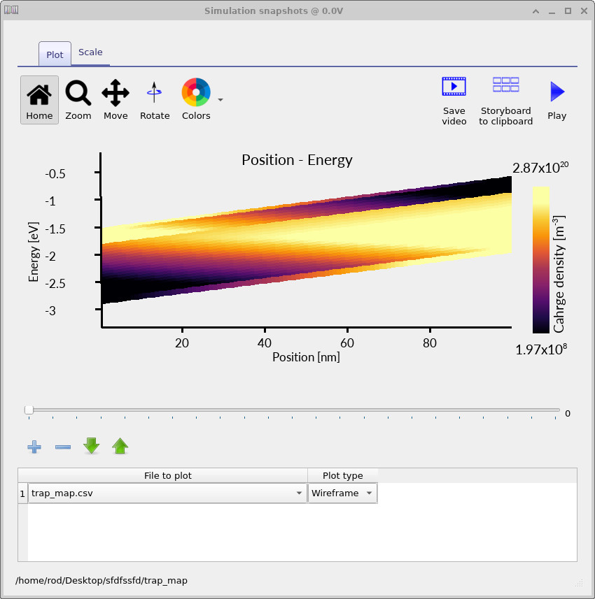
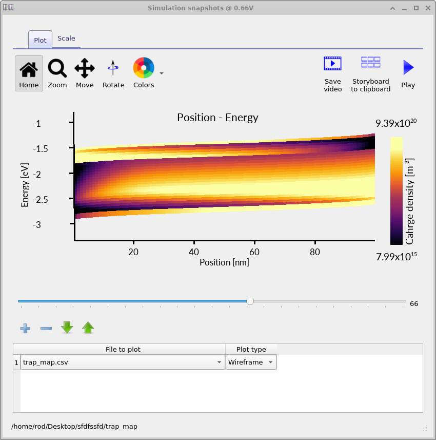
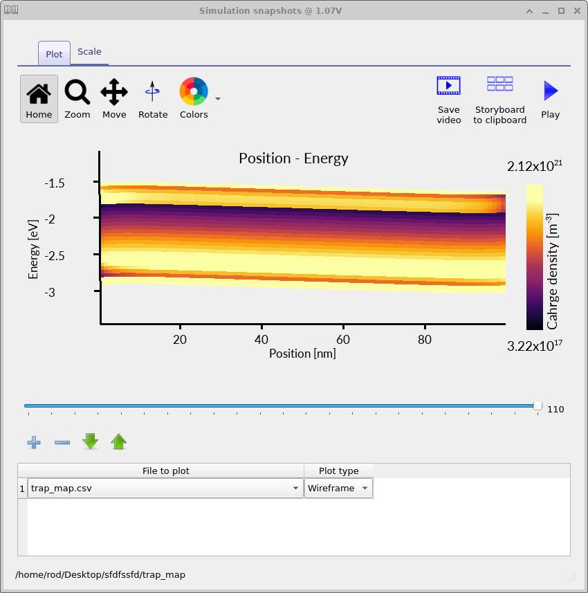
The trap map makes the distributed nature of the model explicit. The charge is not placed into a single defect level; instead, the occupied density is spread across a finite energy range and varies with position inside the device. This is one of the key reasons distributed trap-state models are useful for disordered semiconductors: they allow energetic disorder, trap filling and spatial electrostatics to be analysed together.
11. Outputting the trap occupation at a single mesh point
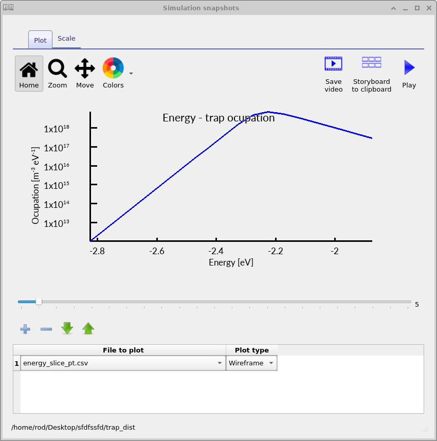
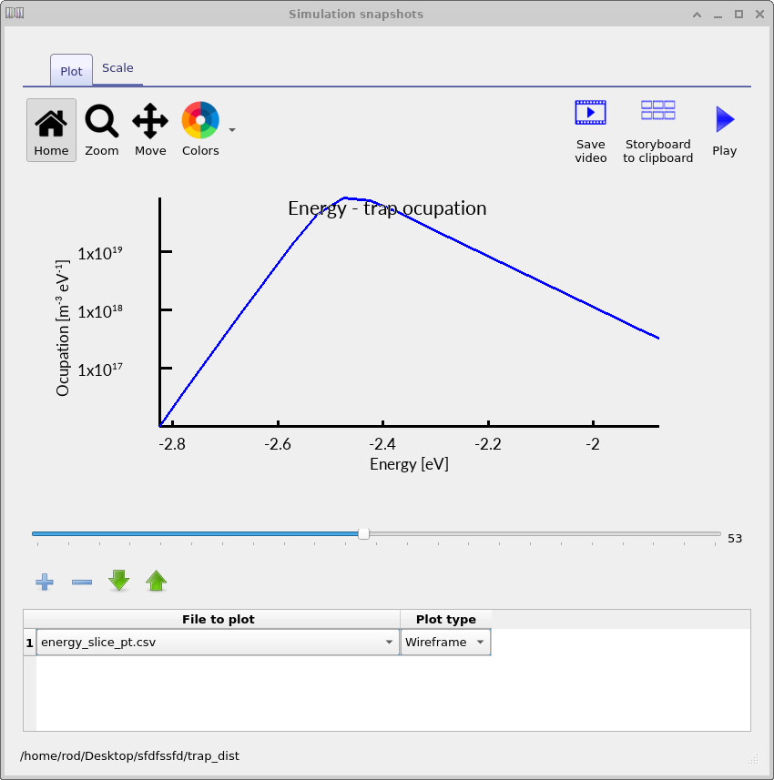
The full energy-space trap map is useful for visualising the entire device, but it can sometimes be easier to understand the physics by examining the trap occupation at one selected spatial position. To do this, reopen the JV editor and change Dump trap distribution from Energy space map to Single mesh point, as shown in ??. Set the y-position to 50. OghmaNano will then output the trap occupation spectrum at the 50th mesh point within the device.
Rerun the simulation.
Inside the trap_map output directory, OghmaNano will now write files such as energy_slice_nt.csv for electron traps and energy_slice_pt.csv for hole traps.
These files contain the occupied trap density as a function of energy at the selected spatial position.
By moving through the voltage slider, you can observe how the energetic distribution of trapped charge evolves during the JV scan.
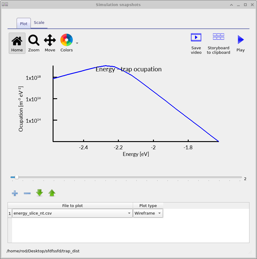
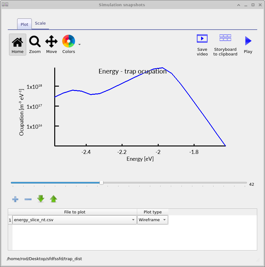
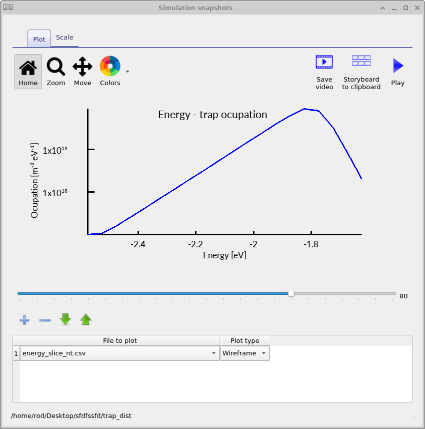
The electron-trap occupation spectra shown in ??, ?? and ?? show how the trap occupation evolves as the applied voltage increases. At low voltage, only a relatively small fraction of the trap distribution is occupied. As the voltage rises, the carrier density increases and progressively fills a larger energetic region of the density of states. The occupation maximum also shifts in energy because the local quasi-Fermi level moves through the trap distribution as charge accumulates inside the device.
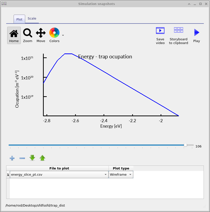
The corresponding hole-trap spectra shown in ??, ?? and ?? show the same physical process from the HOMO side of the density of states. As the device is driven forward and the carrier density increases, the occupied trap density grows and shifts through the HOMO-side trap distribution in exactly the same way as for the electron traps.
These one-dimensional energy slices are particularly useful because they separate the energetic part of the problem from the spatial part. The full trap map shows where charge is stored within the device, while the single-mesh-point spectra show exactly how that charge is distributed in energy. Together, these outputs provide a direct visualisation of trap filling, quasi-Fermi-level motion and charge storage inside a disordered semiconductor device.
12. Adding a deep Gaussian recombination-active trap
The complex density-of-states editor allows several analytical functions to be combined into the same trap distribution. This means the density of states does not need to consist only of a pure exponential tail or a pure Gaussian distribution. Instead, several functions can be superimposed to build more realistic disordered density-of-states models containing both shallow tail states and deeper localised trap bands.
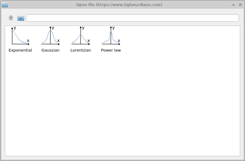
To add another component to the LUMO-side density of states, click the + button in the LUMO panel of the complex DOS editor. You can type the analytical expression directly into the function field, or click the three-dot button to open the equation selector shown in ??. The equation selector contains several predefined density-of-states functions including exponential, Gaussian, Lorentzian and power-law distributions.
In this example, the LUMO-side density of states contains two enabled functions. The first is the original exponential tail, while the second is a Gaussian deep trap:
\[ \rho_\mathrm{G}(E)= a\exp\left[ -\left( \frac{c+E-E_C} {\sqrt{2}\,b} \right)^2 \right]. \]
The parameter a controls the density scale, b controls the energetic width of the Gaussian, and c shifts the trap away from the band edge. In this example, c = 0.7 eV, placing the Gaussian trap deep inside the bandgap relative to the LUMO transport level. The HOMO-side density of states is left as a simple exponential tail.
Physically, this model represents a semiconductor containing both shallow energetic disorder and a deeper defect band. The shallow exponential tail mainly controls transport and trapping close to the transport level, while the deep Gaussian state acts as a strong recombination and charge-storage centre. Since each function has its own enable switch, the effect of the deep trap can be isolated without changing the rest of the device model.
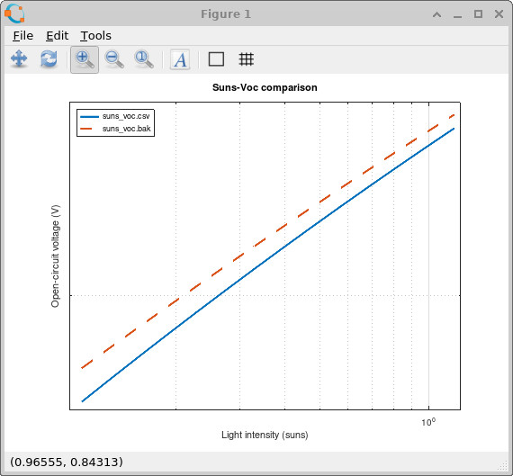
To investigate the effect of the deep trap on recombination, run a Suns Voc simulation. Open the Simulation type ribbon and select Suns Voc, as shown in ??. Then run the simulation from the main window using the blue run button or by pressing F9.
When the simulation has finished, the file suns_voc.csv will contain the open-circuit voltage as a function of illumination intensity.
Make a backup copy of this file using Windows Explorer and rename it to suns_voc.bak.
Then return to the complex DOS editor and disable the Gaussian deep-trap row while leaving the exponential tail enabled.
Run the Suns–Voc simulation again.
The new suns_voc.csv file now corresponds to the device without the deep Gaussian trap, while suns_voc.bak contains the simulation with the deep trap included.
Plotting these two files together gives the comparison shown in
??.
The deep Gaussian trap reduces the open-circuit voltage because it introduces an additional recombination pathway deep inside the bandgap. This reduces the quasi-Fermi-level splitting established under illumination and therefore lowers the achievable VOC. The effect is particularly strong at lower light intensities where trap-assisted recombination dominates the carrier dynamics.
Suns–Voc measurements are therefore extremely useful for distinguishing shallow energetic disorder from deeper recombination-active defect states. Since the device is measured under open-circuit conditions, the experiment isolates the internal recombination physics without the additional complication of carrier extraction current.
If you would like to plot the Suns–Voc comparison shown in
??,
you can use either the MATLAB/Octave or Python scripts below.
These scripts compare suns_voc.csv against suns_voc.bak and plot the open-circuit voltage as a function of light intensity.
MATLAB / Octave version
clear;
close all;
clc;

% Load data
voc     = load('suns_voc.csv');
voc_bak = load('suns_voc.bak');
Show full MATLAB script
clear;
close all;
clc;

% Load data
voc     = load('suns_voc.csv');
voc_bak = load('suns_voc.bak');

% ============================================
% Figure : Suns-Voc
% ============================================

figure;

loglog(voc(:,1), abs(voc(:,2)), ...
    'LineWidth', 2);

hold on;

loglog(voc_bak(:,1), abs(voc_bak(:,2)), '--', ...
    'LineWidth', 2);

grid on;
box on;

xlabel('Light intensity (suns)');
ylabel('Open-circuit voltage (V)');

title('Suns-Voc comparison');

legend( ...
    'suns\_voc.csv', ...
    'suns\_voc.bak', ...
    'Location', 'northwest' ...
);
Python version
import numpy as np
import matplotlib.pyplot as plt

# Load data
voc = np.loadtxt("suns_voc.csv")
voc_bak = np.loadtxt("suns_voc.bak")
Show full Python script
import numpy as np
import matplotlib.pyplot as plt

# Load data
voc = np.loadtxt("suns_voc.csv")
voc_bak = np.loadtxt("suns_voc.bak")

# ============================================
# Figure : Suns-Voc
# ============================================

plt.figure()

plt.loglog(voc[:,0], np.abs(voc[:,1]),
           linewidth=2)

plt.loglog(voc_bak[:,0], np.abs(voc_bak[:,1]),
           '--',
           linewidth=2)

plt.grid(True)

plt.xlabel("Light intensity (suns)")
plt.ylabel("Open-circuit voltage (V)")

plt.title("Suns-Voc comparison")

plt.legend([
    "suns_voc.csv",
    "suns_voc.bak"
], loc="upper left")

plt.show()
Summary
This tutorial has shown how trap states can be included explicitly in a disordered semiconductor device model. Rather than treating recombination as arising from a single isolated SRH defect level, OghmaNano allows the trap density of states to be described as an energetic distribution. This is essential for organic semiconductors, amorphous silicon, oxide semiconductors and other thin-film materials where localized states extend through the bandgap and strongly influence the relation between carrier density, quasi-Fermi-level position, recombination and mobility. Although the practical example uses a PM6:Y6 organic solar cell, the aim of the tutorial is broader: to show how distributed trap states are represented, solved and diagnosed in disordered semiconductor device simulations.
Starting from a PM6:Y6 organic solar-cell simulation, we compared shallow and broad exponential trap-tail distributions under both dark and illuminated conditions. Broadening the trap distribution changed the dark JV curve, the illuminated JV curve and the total stored charge because the device could occupy a wider range of localized states. The trap-map outputs then made this behaviour visible directly, showing how the occupied trap population varies with position, energy and applied voltage.
Finally, a deep Gaussian trap was added on top of the exponential tail to demonstrate how complex density-of-states models can represent both shallow energetic disorder and deeper recombination-active defects. The Suns–Voc simulation showed that such deep states can reduce the open-circuit voltage by increasing trap-assisted recombination and reducing the quasi-Fermi-level splitting under illumination. Overall, the tutorial demonstrates that trap distributions are not a minor correction in disordered semiconductor simulations: they are often central to obtaining physically meaningful JV curves, charge densities, recombination rates and photovoltaic performance.
Next steps: If you want to explore the wider modelling framework around this tutorial, the following pages are good places to continue.
- What are organic semiconductors? Materials, devices and applications — a broader introduction to the materials and device classes where trap states are important.
- Organic semiconductor device modelling: OPVs, OLEDs and OFETs — an overview of how drift-diffusion, recombination and optical models are used for organic devices.
- Organic solar cell (OPV) simulation — a practical starting point for simulating organic photovoltaic devices in OghmaNano.
- Organic field-effect transistor (OFET) simulation — useful if you want to see how trap filling and charge transport appear in transistor geometries.
- Space-Charge Limited Current (SCLC) example — a useful follow-on for understanding injection, mobility and trap-limited transport.
- Simulating bulk-heterojunction morphologies with 2D electrical slices — a more advanced tutorial showing how morphology and transport interact in organic solar cells.
- Why trap states are needed in disordered semiconductor models — the underlying physical argument for why trap distributions are required to obtain realistic carrier densities, recombination rates, mobilities and J–V curves.