Photonic Crystal Tutorial: Simulate a Photonic Crystal and Waveguide
A photonic crystal is a structure whose refractive index varies periodically on the scale of the wavelength of light — for example a regular array of dielectric pillars. Just as the periodic atomic lattice of a semiconductor opens an electronic band gap, the periodic optical lattice of a photonic crystal opens a photonic band gap: a range of wavelengths that simply cannot propagate through it. If you then introduce a deliberate defect, such as removing a line of pillars, light whose wavelength lies inside the band gap becomes trapped in that defect and is guided along it — even around tight corners. This is a photonic crystal waveguide, and it is the building block of integrated photonic circuits, filters and sensors.
In this tutorial you will build a photonic crystal in OghmaNano, run a full FDTD (finite-difference time-domain) simulation, watch the optical field move through the structure, and measure how much light gets through as a function of wavelength. You will then tune the geometry to shift the photonic band, and finally carve a defect into the lattice to make a guided waveguide.
Step 1: Launch OghmaNano
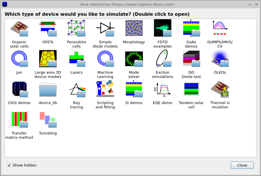
Start OghmaNano from the Windows Start menu, then click New simulation to open the library of available device types, shown in ??.
Step 2: Create a new photonic crystal simulation
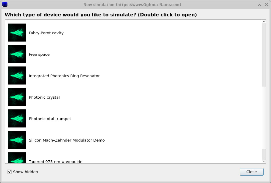
In the New simulation window (??) double-click FDTD examples. This opens the list of optical/FDTD templates shown in ??, which includes a Fabry–Perot cavity, free space, an integrated photonics ring resonator, a Mach–Zehnder modulator and several waveguides. For this tutorial double-click Photonic crystal. When prompted, save the simulation to a folder you have write access to.
💡 Tip: For best performance save to a local drive such as
C:\. Simulations stored on network, USB, or cloud folders
(e.g. OneDrive) can run slowly due to heavy read/writes.
Step 3: Run the simulation
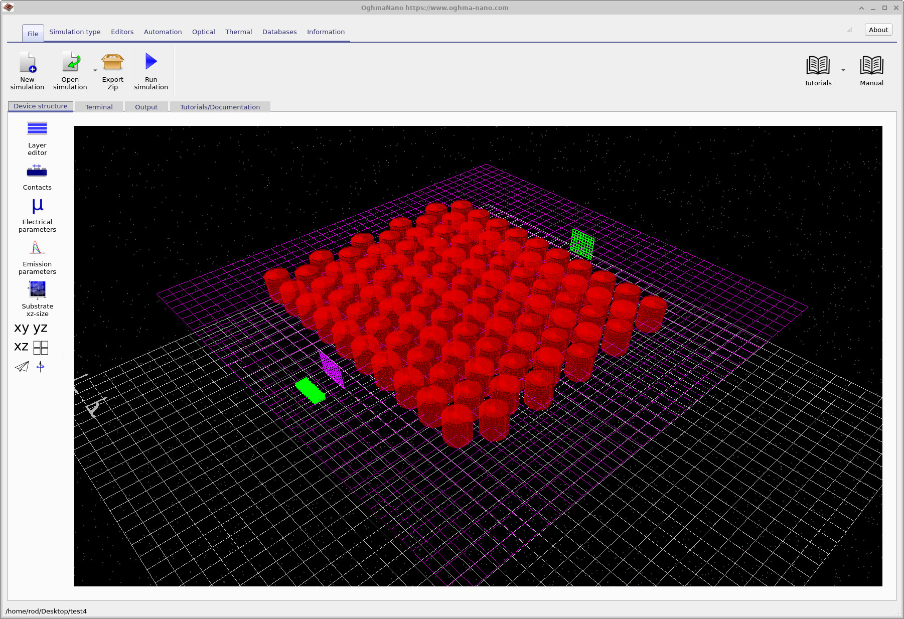
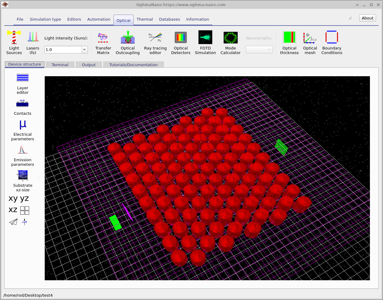
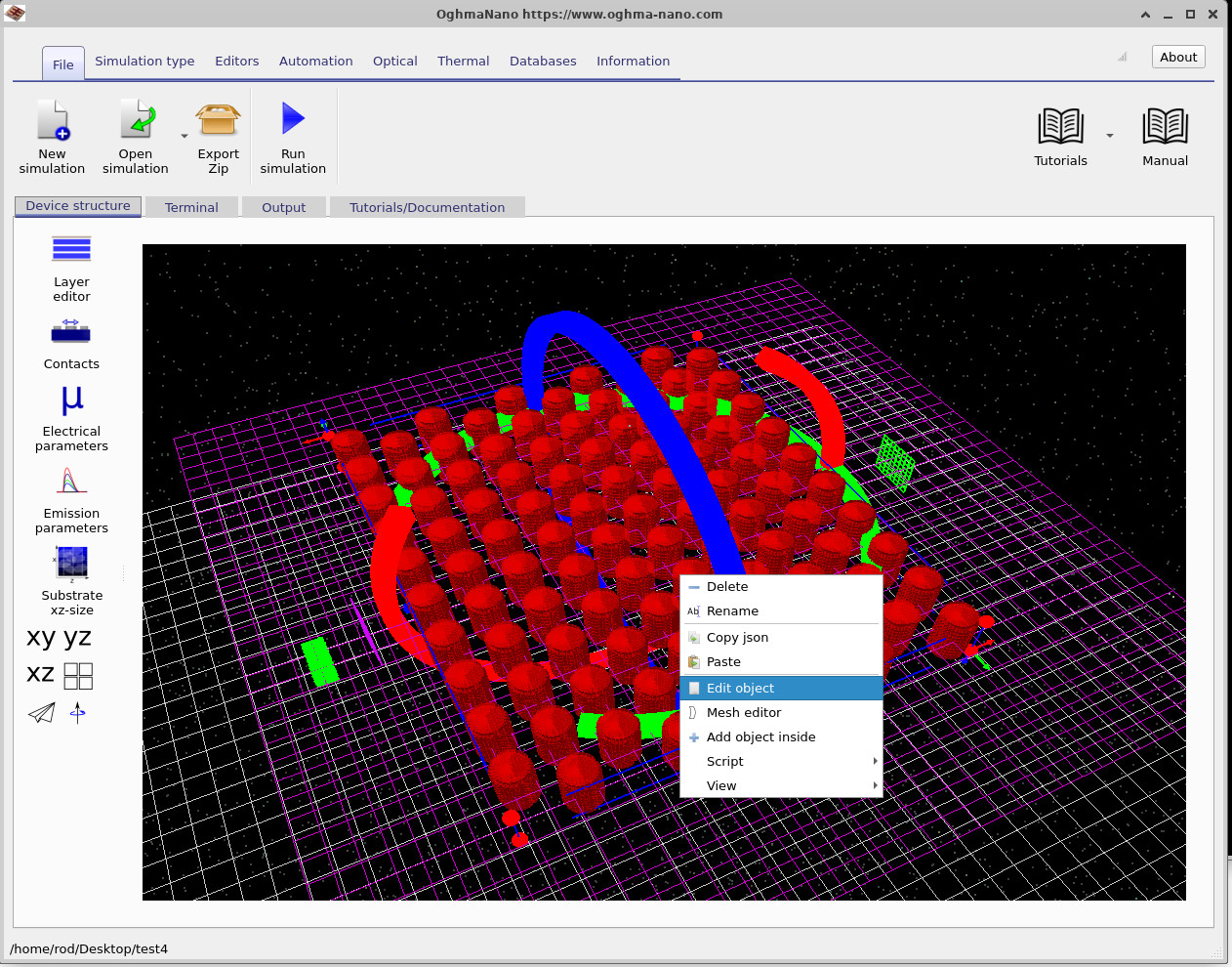
Once saved, the main window opens (see ??). The device is an array of dielectric pillars (the red tubes) sitting between two thin detector planes: a purple input detector near the source and a green output detector on the far side. Use the xy/yz/xz buttons to orient the view. Click Run simulation (the blue play icon) or press F9. On slower machines the FDTD calculation may take a little while.
When the run finishes, open the Output tab (??) to browse the files the solver has written. Double-clicking any file opens it in the appropriate viewer.
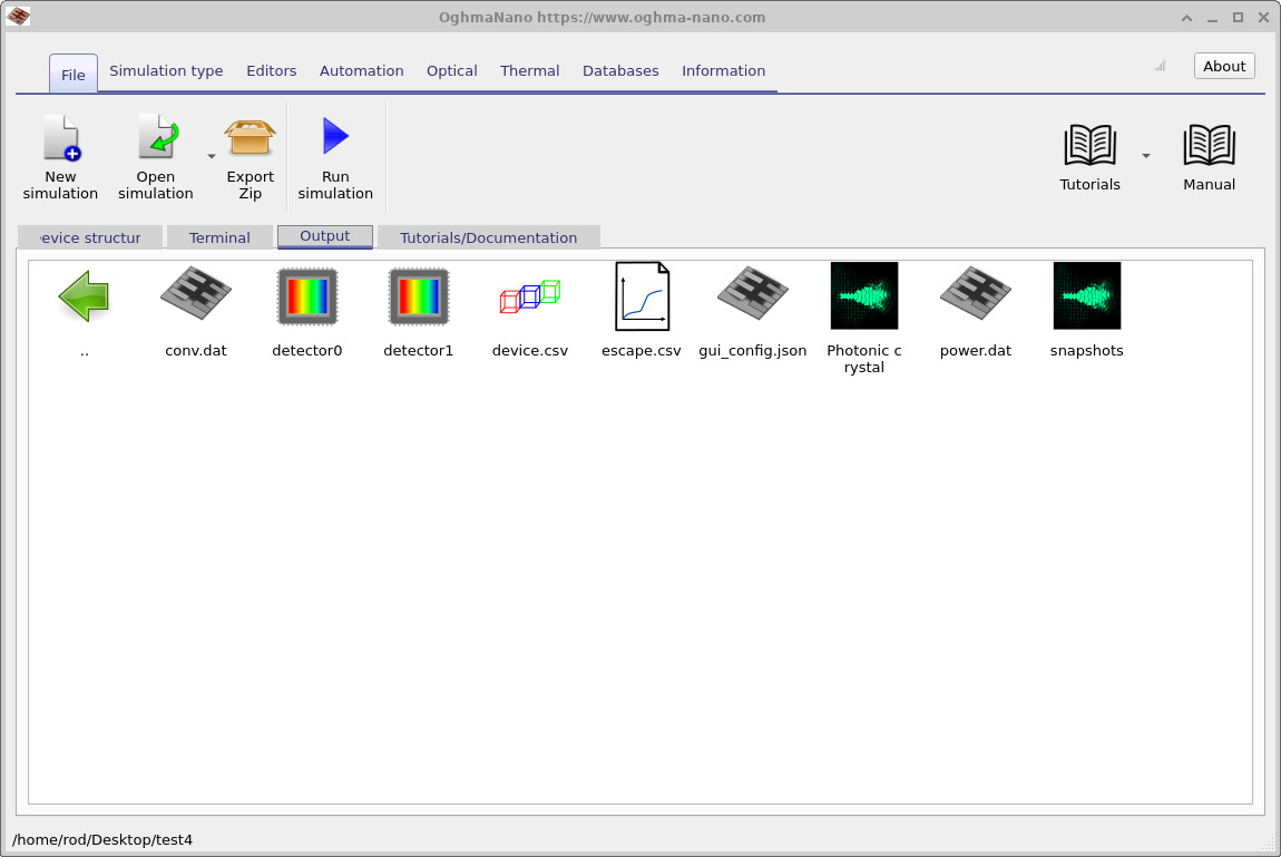
snapshots folder (time snapshots of the field), and the detector0 and detector1 folders, which hold the spectra recorded by the input and output detectors.
Double-clicking a file or folder opens it.
Step 4: Watch the field propagate
Double-click the snapshots folder to open the snapshot viewer (??).
The plotted file is Ey.csv — one component of the electric field — shown as a coloured wireframe surface, where colour and height both encode the field strength in V/m.
Drag the slider underneath the plot to step through time. You will see the launched pulse spread out from the source on the left, strike the photonic crystal, and partially scatter and transmit through it. Watching the field evolve is the most intuitive way to confirm the simulation is doing what you expect before you trust the numbers.
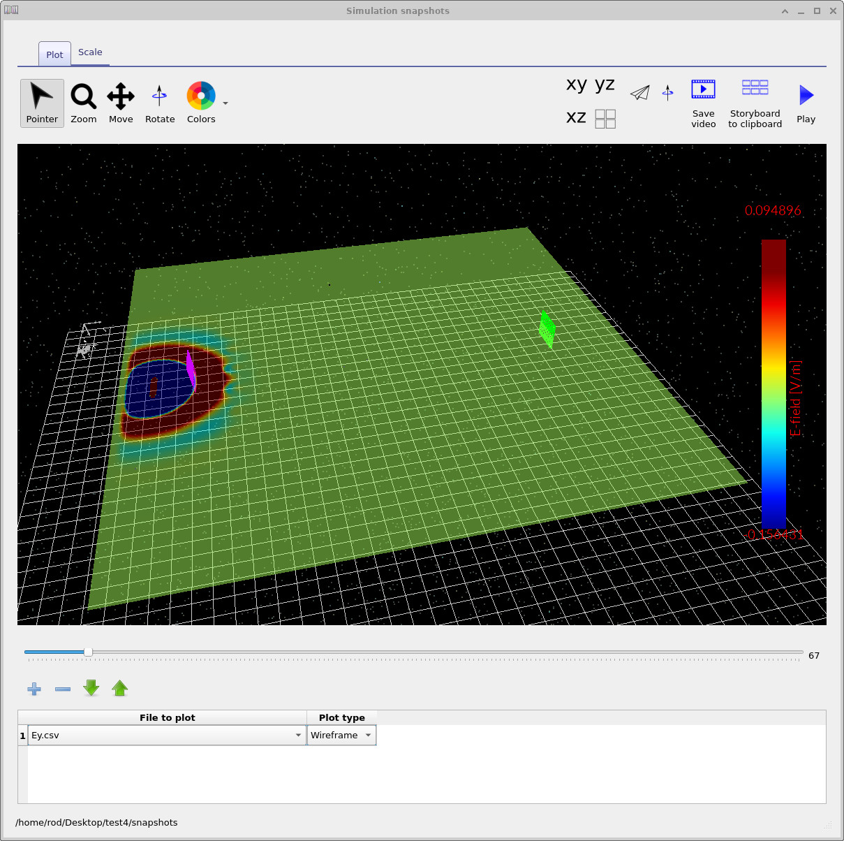
Ey.csv as a wireframe.
The colour bar gives the electric field in V/m.
Use the slider at the bottom to move through time and watch the pulse propagate towards, and through, the photonic crystal.
Step 5: Detectors and the transmission spectrum
Now look at what the two detectors recorded. From the Output tab open the detector0 and detector1 folders; each contains a file called lam_E.csv, which is the wavelength-resolved field intensity |E|2 arriving at that detector.
The two detectors are the purple and green grids you can see in the device view.
Opening lam_E.csv in detector0 gives the input spectrum (??): this is the broadband pulse launched at the structure, with most of its energy around 900 nm.
Opening lam_E.csv in detector1 gives the output spectrum (??), plotted on a logarithmic axis. Notice how heavily the light is attenuated at most wavelengths — the photonic crystal blocks them.
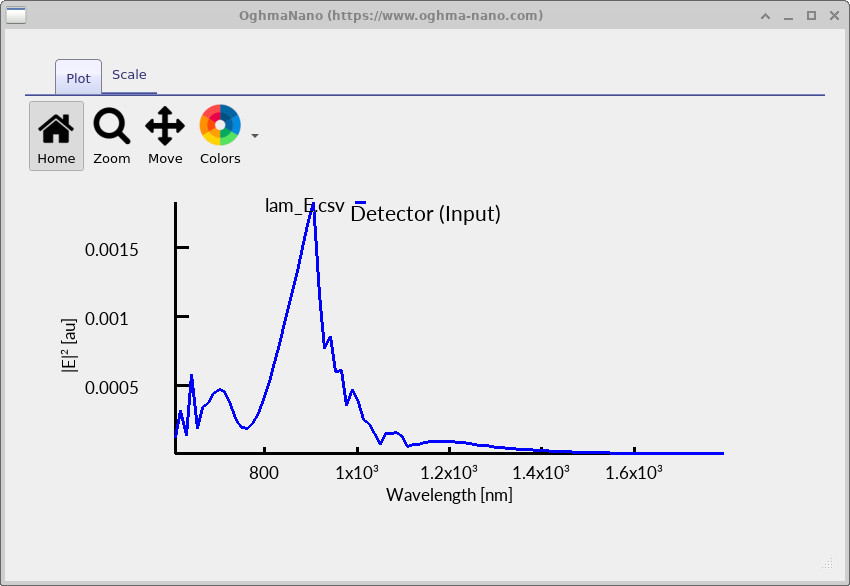
detector0/lam_E.csv): the broadband pulse incident on the crystal, peaking near 900 nm. This is the reference against which the output is compared.
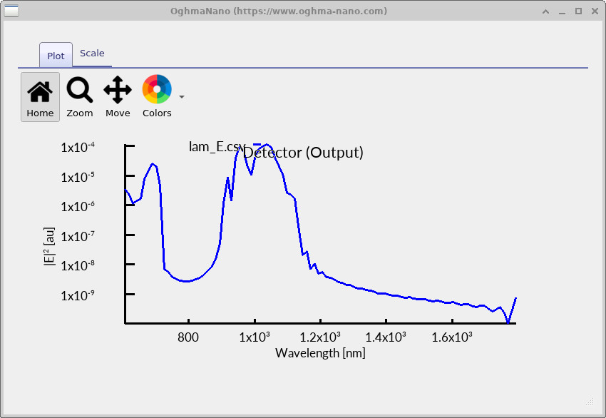
detector1/lam_E.csv) on a log scale. Most wavelengths are suppressed by several orders of magnitude because they fall inside the photonic band gap.
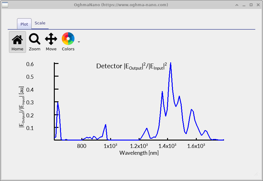
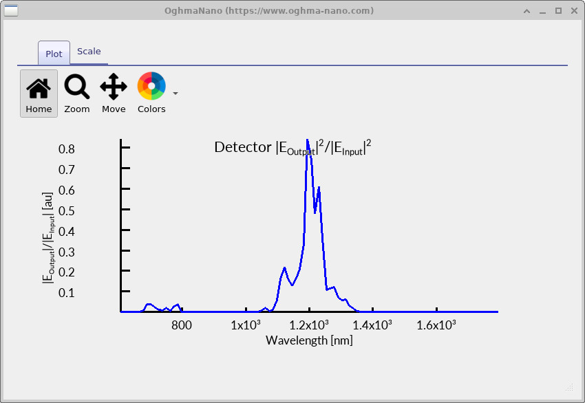
Comparing two raw spectra by eye is awkward, so the detector folder also contains lam_norm.csv, the ratio |EOutput|2/|EInput|2. This is the transmission spectrum of the photonic crystal. Double-click it to obtain ??.
The clear peak just above 1000 nm is the band of wavelengths the photonic crystal lets through; the strongly suppressed regions on either side are the photonic band gap, where propagation is forbidden. In other words, this single curve tells you both what the crystal transmits and where its band gap sits.
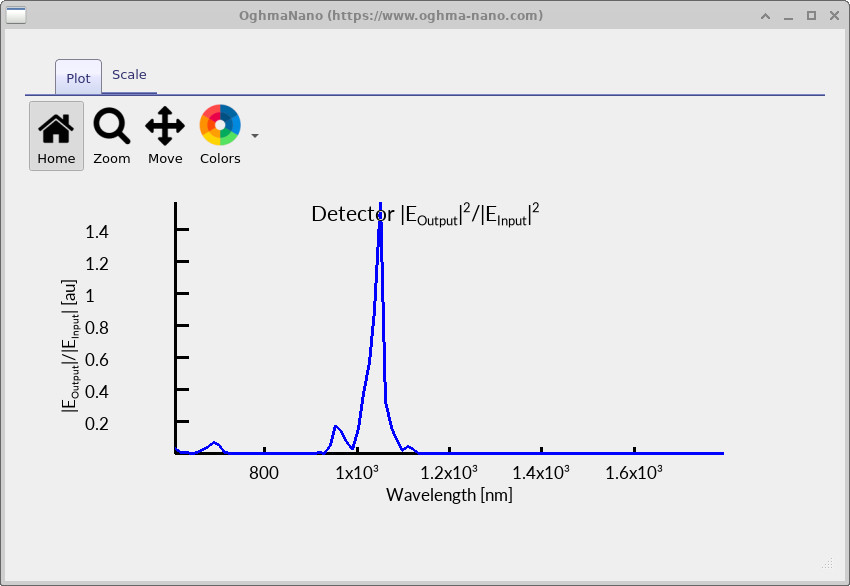
lam_norm.csv.
The peak just above 1000 nm marks the wavelengths the photonic crystal transmits; the suppressed wavelengths lie inside the photonic band gap.
Step 6: Tuning the pillar radius
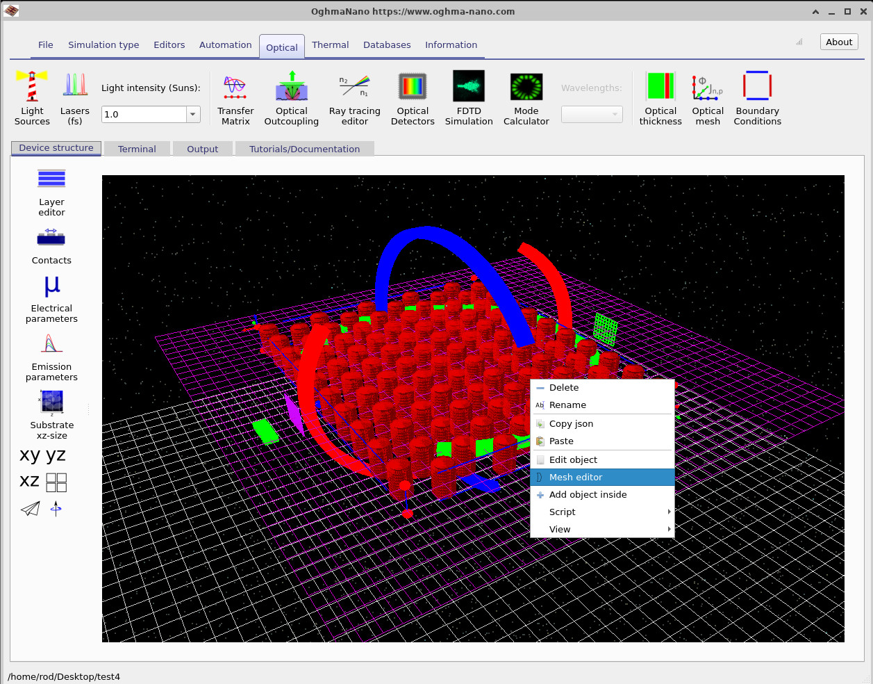
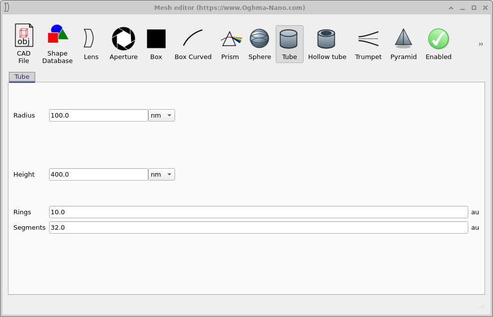
The position of the band gap is set by the geometry of the lattice. To see this, right-click on the photonic crystal in the device view and choose Mesh editor from the menu (??). The mesh editor (??) lets you change the shape that is repeated to build the crystal — here a tube with a radius of 100 nm, a height of 400 nm, and a chosen number of rings and segments controlling how finely it is meshed.
Change the radius to 150 nm and the pillars visibly thicken in the device view (??). Re-run the simulation and reopen lam_norm.csv to obtain the new transmission spectrum (??).
Now try a radius of 120 nm. The transmission peak (??) lands near 1200 nm — neatly between the 100 nm and 150 nm results. The trend is consistent and physically meaningful: fatter pillars put more high-index material into each unit cell, which raises the effective refractive index and scales the photonic bands to longer wavelengths. By choosing the radius you are effectively dialling the band gap to where you want it.
Step 7: Building a photonic crystal waveguide
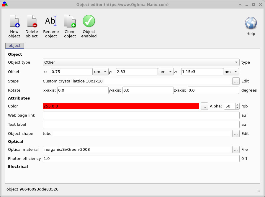
So far the lattice has been generated for you. To see how, and to take control of it, right-click the photonic crystal and choose Edit object (??). The object editor (??) collects everything about the object: its position, the tube shape, its optical material (here silicon), and — on the Steps row — the rule that stamps the shape out into a lattice.
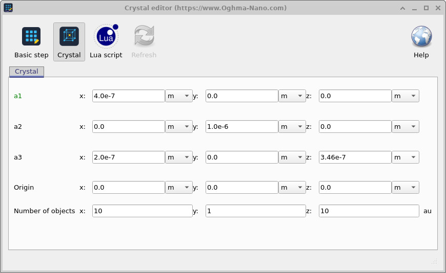
Clicking the … button on the Steps row opens the step editor. On the Crystal tab (??) the lattice is defined by three vectors and a count. Here a1 = (400 nm, 0, 0) sets a 400 nm pitch along x, a2 = (0, 1 µm, 0) is the single layer in y, and a3 = (200 nm, 0, 346 nm) offsets each row by half a pitch — a 200 nm shift with a 346 nm = 400 nm × √3/2 spacing — which produces the familiar triangular (hexagonal) close-packed arrangement. The crystal is repeated 10 × 1 × 10 times.
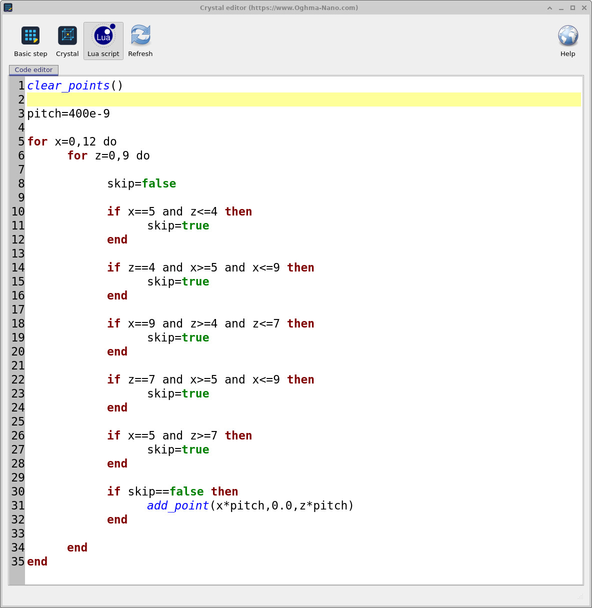
clear_points() and add_point(), and everything is in metres.
The regular lattice is the easy case, but it is not the only one. Click the Lua script button and the editor switches to code (??). Here the pillar positions are generated programmatically. There are only two commands you need: clear_points() wipes any existing positions, and add_point(x, y, z) places one pillar — always in metres. Wrapped in a couple of nested loops, this lets you build any shape you like.
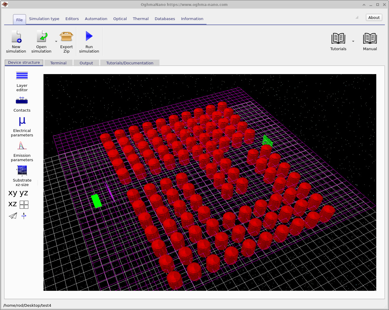
The script in ?? lays down a 13 × 10 grid on a 400 nm pitch, but a handful of if conditions set skip=true for selected pillars so they are never added. Those missing pillars form a defect channel through the lattice — in this case a U-shaped (bracket) bend. Applying the script produces the waveguide shown in ??.
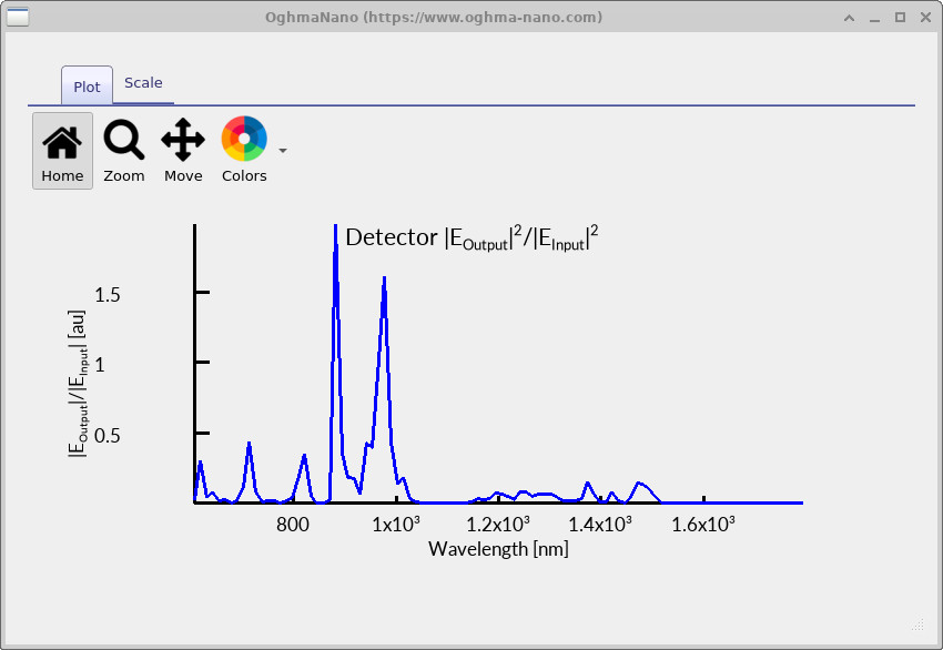
Re-run the simulation and reopen lam_norm.csv. The transmission spectrum of the waveguide (??) now shows several sharp peaks rather than one broad band: these are the guided modes that the bent channel supports inside the band gap. Light at those wavelengths is steered around the corner and reaches the output detector; everything else is rejected by the lattice.
Nice! You’ve run your first photonic crystal simulation, measured its transmission, tuned its band gap, and built a working photonic crystal waveguide.
The output from your simulation
Each FDTD run produces a collection of outputs that capture different aspects of the optical behaviour — from time snapshots of the field, to the spectra recorded by each detector, to the geometry of the device itself. These files are usually plain csv files which can be opened directly in OghmaNano’s built-in viewers or processed externally (for example, plotting data in Excel or Python). The most important outputs for this photonic crystal study are summarised in Table 1 below.
| File name | Description |
|---|---|
| detector0/lam_E.csv | Input spectrum |E|2 vs wavelength (purple detector) |
| detector1/lam_E.csv | Output spectrum |E|2 vs wavelength (green detector) |
| detectorN/lam_norm.csv | Transmission |Eout|2/|Ein|2 vs wavelength |
| snapshots/ | Time snapshots of the field (e.g. Ey.csv); see ?? |
| device.csv | 3D device / geometry model |
| escape.csv | Energy escaping the simulation domain |
| power.dat | Field power vs time |
| conv.dat | Convergence of the FDTD solver |
| gui_config.json | Saved view/plot settings; see ?? |
👉 Next steps:
- Explore the other FDTD examples, such as the ring resonator and Mach–Zehnder modulator, to see different ways of routing light on a chip.
- Return to the introduction to optical simulation for a broader overview of the FDTD method in OghmaNano.