

Simulating a GaAs/AlGaAs Heterojunction Solar Cell
1. Introduction: GaAs solar cells and their applications

Gallium arsenide (GaAs) solar cells are used in applications where high conversion efficiency, low weight and reliability are more important than cost. GaAs is a direct-bandgap semiconductor with a bandgap of approximately 1.42 eV, allowing sunlight to be absorbed efficiently within a few micrometres of material. This makes it particularly attractive for high-performance photovoltaic devices.
GaAs-based solar cells are widely used in satellites and spacecraft, where available surface area is limited and radiation tolerance is important (??). They are also used in concentrator photovoltaics, where sunlight is focused onto a small semiconductor cell, and in specialist applications such as high-altitude aircraft and laser power converters. Modern space solar cells often combine GaAs with other III–V semiconductors in multijunction structures to achieve higher efficiencies.
In this tutorial, we simulate a GaAs/AlGaAs heterojunction solar cell. A thin, wider-bandgap AlGaAs window is placed above the GaAs junction to reduce unwanted absorption and surface recombination losses. Using OghmaNano, we examine how the device absorbs sunlight, transports photogenerated carriers and produces electrical power, combining optical transfer-matrix calculations with drift–diffusion modelling.
2. Creating and understanding the GaAs/AlGaAs solar cell
We will simulate a GaAs/Al0.3Ga0.7As heterojunction solar cell, consisting of a thin, wide-bandgap AlGaAs window above a GaAs p–n junction. Although relatively simple, this device illustrates several important aspects of III–V photovoltaics, including optical absorption, charge-carrier generation, drift–diffusion transport, recombination and the influence of semiconductor heterojunctions on carrier collection.
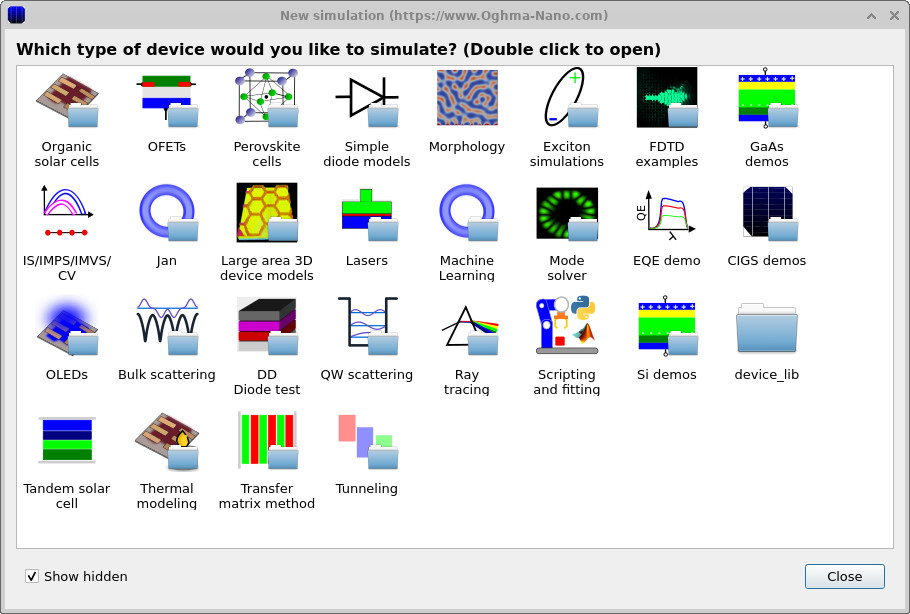
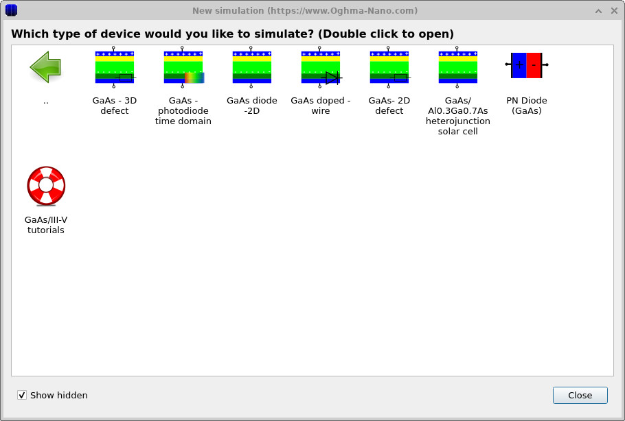
To begin, start OghmaNano and click New simulation in the File ribbon. This opens the device library (??). Double-click GaAs demos to open the available GaAs simulations (??). Select GaAs/Al0.3Ga0.7As heterojunction solar cell, choose a destination folder and click Save.
Once loaded, OghmaNano displays the device in the Device structure tab (??). The green arrows indicate illumination from above, while the coloured regions represent the four semiconductor layers. The structure and material properties can be modified using the layer editor and electrical parameter editor.
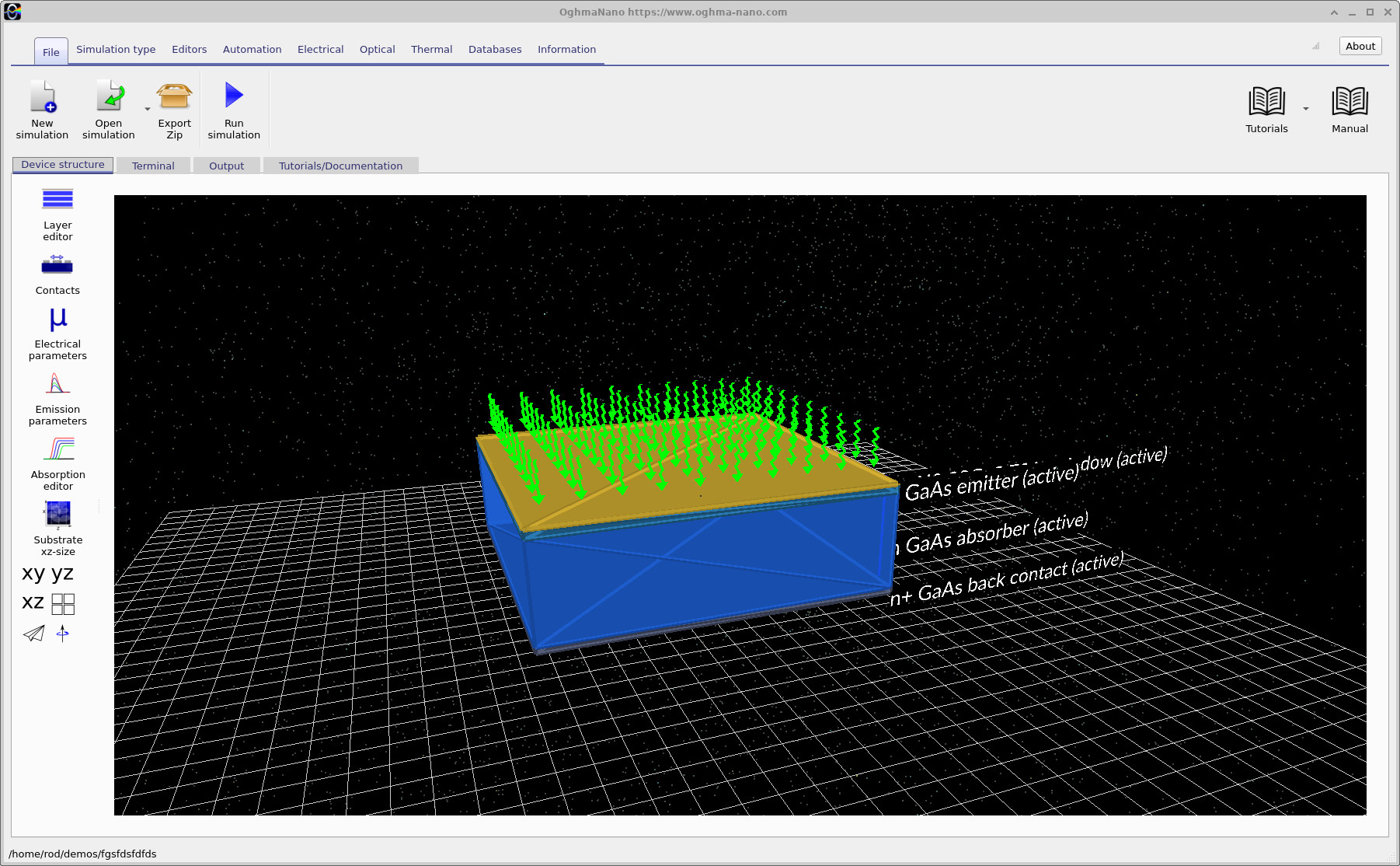
The device consists of four semiconductor layers, arranged from the illuminated surface to the back contact:
| Layer | Material | Thickness | Doping (m⁻³) |
|---|---|---|---|
| p+ window | Al0.3Ga0.7As | 35 nm | 1 × 1024 (acceptors) |
| p emitter | GaAs | 200 nm | 2 × 10²³ (acceptors) |
| n absorber | GaAs | 2.5 µm | 2 × 10²² (donors) |
| n+ back contact | GaAs | 150 nm | 1 × 1024 (donors) |
The GaAs absorber is responsible for converting incident photons into electron–hole pairs. GaAs has a direct bandgap of approximately 1.42 eV, giving it a high absorption coefficient and allowing sunlight to be absorbed within a relatively thin semiconductor layer. The p-type emitter and n-type absorber form the primary photovoltaic junction. Carrier diffusion across this junction establishes a depletion region and a built-in electric field, which helps separate photogenerated electrons and holes and transport them towards their respective contacts. The Al0.3Ga0.7As window introduces a semiconductor heterojunction at the illuminated surface. Adding aluminium increases the bandgap relative to GaAs, making the window more transparent to photons that can be absorbed in the underlying GaAs. The difference in electron affinity and bandgap also produces conduction- and valence-band discontinuities at the interface. These can help suppress minority-carrier transport towards the front surface, reducing recombination losses, although excessively large band offsets can impede carrier extraction. The heavily doped p+ window and n+ back-contact layer also help provide low-resistance electrical connections. At the rear, the transition between the lightly doped absorber and heavily doped contact creates an additional electric field that can repel minority holes from the back contact. The combination of layer thickness, doping and band alignment therefore determines how efficiently absorbed photons are converted into electrical current.
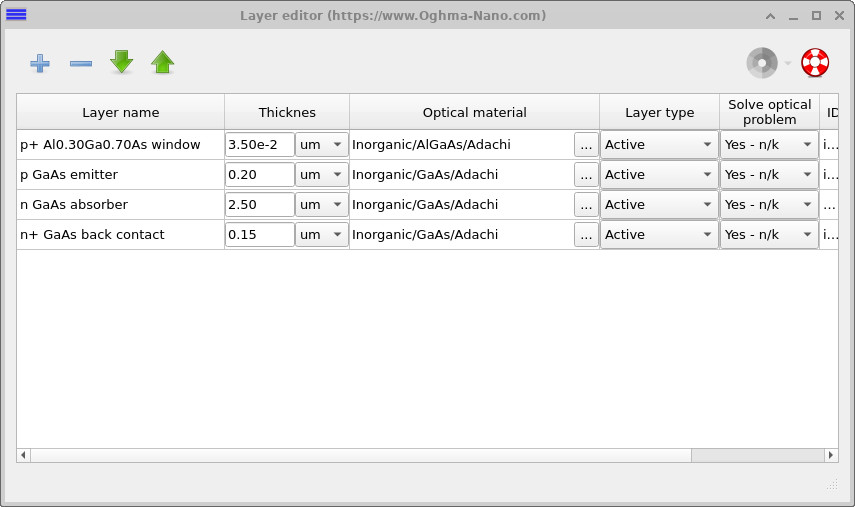
The device structure can be examined and modified by clicking the Layer editor button on the left-hand side of the Device structure tab in the main window. The button is represented by three coloured horizontal bars depicting a layered device. This opens the Layer editor (??), where the thickness, optical material and type of each layer can be changed. Layer thickness is particularly important in solar cells because it determines how much light is absorbed and how far photogenerated carriers must travel before reaching the contacts.
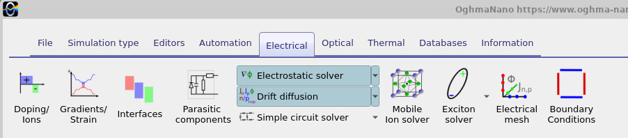
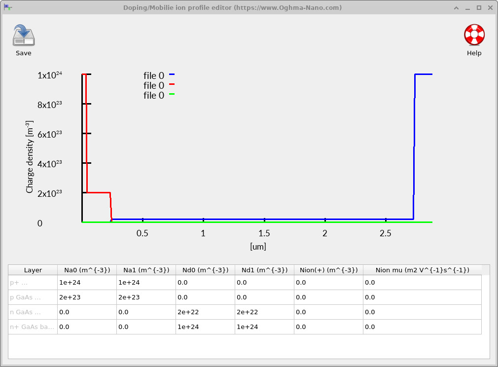
The Electrical ribbon (??) provides access to the Doping/Ions and Gradients/Strain editors. The doping editor (??) controls the donor and acceptor concentrations throughout the device. These determine the position and width of the depletion region, the built-in electric field and the electrical conductivity of each layer. Consequently, changing the doping can significantly influence carrier collection, recombination and the resulting J–V characteristics.
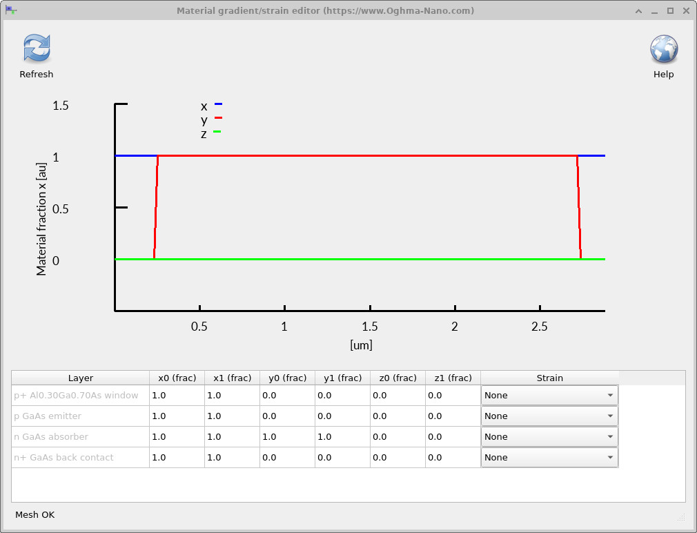
The Gradients/Strain editor (??) controls the material composition variables \(x\), \(y\) and \(z\). These can be specified independently at the beginning and end of each layer, allowing both uniform and compositionally graded semiconductor structures to be simulated. For alloys such as AlxGa1-xAs, the aluminium fraction influences the bandgap and band alignment with GaAs. Changing the alloy composition therefore provides a way to investigate how heterojunction band offsets affect carrier transport and recombination. The interpretation of each composition variable is defined by the selected semiconductor material model.
3. Running the simulation and examining the results
To run the GaAs/AlGaAs solar-cell simulation, click the blue Run simulation button in the File ribbon, or press F9. Open the Terminal tab to follow the calculation (??). At first, the terminal output may look complicated, with many lines of numerical information appearing on the screen. However, the output is relatively straightforward to interpret once you understand what each part represents.
The first stage of the simulation is the optical calculation, shown by the coloured text at the top of ??. OghmaNano calculates optical absorption and photogeneration at different wavelengths across the incident solar spectrum. Once this calculation is complete, the program begins the current–voltage (J–V) sweep, applying a series of voltages across the solar cell and calculating the resulting current density.
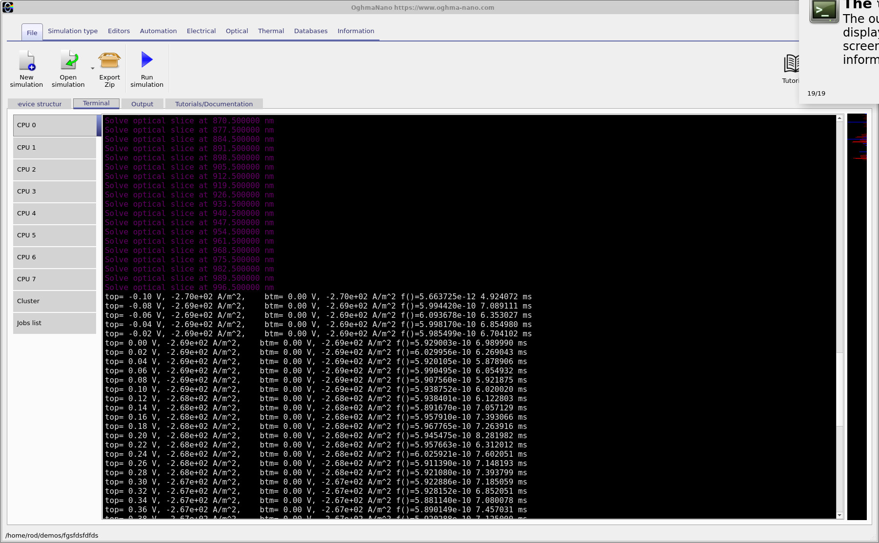
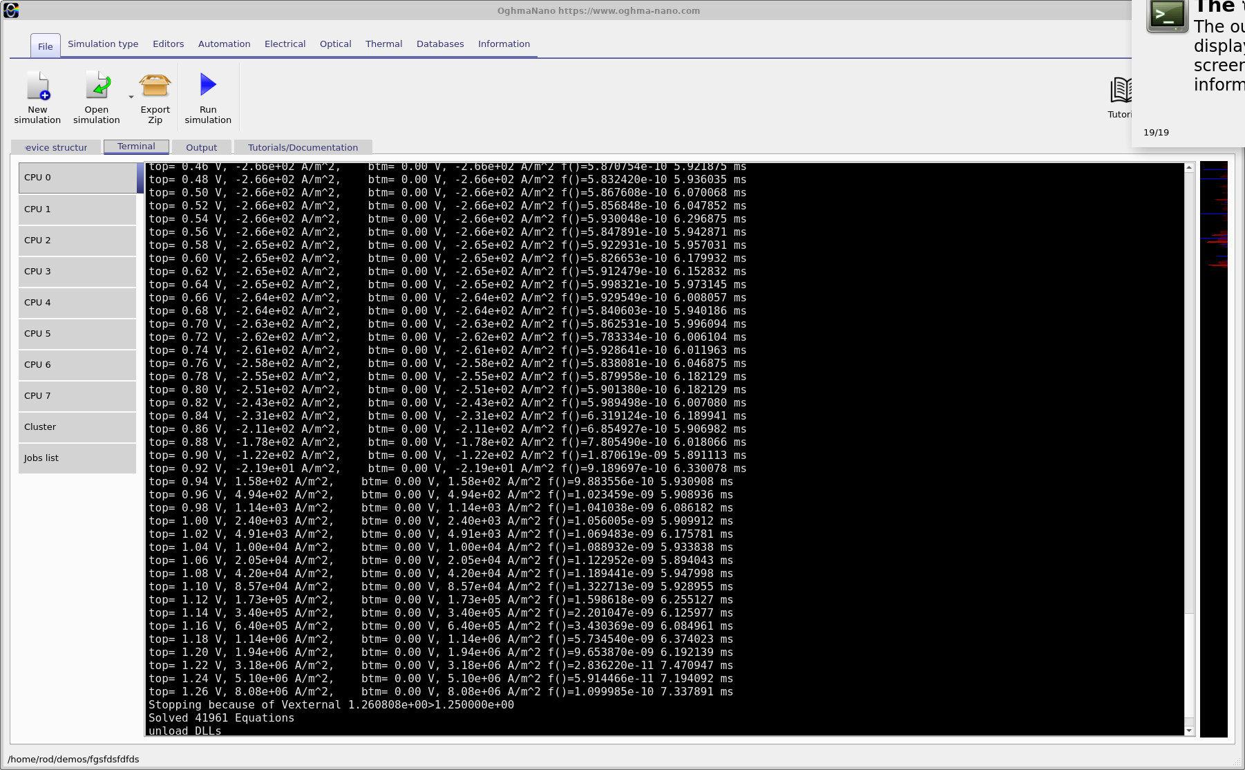
Each line of the J–V calculation corresponds to one applied voltage.
The value labelled top= gives the voltage applied to the
top contact, while btm= gives the voltage at the
bottom contact, which is held at 0 V. The calculated current
density is displayed in A/m² next to the applied voltage.
The quantity f()= is the numerical residual of the electrical
solver, indicating how closely the calculated solution satisfies the
semiconductor equations. Smaller residuals indicate better numerical convergence.
As the applied voltage increases, the photocurrent gradually decreases in magnitude. In ??, the voltage sweep approaches the open-circuit voltage, VOC. Between approximately 0.92 V and 0.94 V, the current density changes from negative to positive, indicating that the net current has passed through zero. This is the open-circuit condition, where the forward diode current exactly balances the photogenerated current. The simulation continues beyond VOC to characterise the forward-bias region of the J–V curve, before stopping when the specified maximum voltage of 1.25 V is exceeded.
At each applied voltage, OghmaNano solves Poisson's equation together with the drift–diffusion and carrier continuity equations. These describe how the electrostatic potential, electron and hole concentrations, and carrier currents vary throughout the device:
\[ \nabla\cdot(\varepsilon\nabla\varphi) = -q\,(p-n+N_D^+-N_A^-) \] \[ \nabla\cdot\mathbf{J}_n = q(R-G), \qquad \nabla\cdot\mathbf{J}_p = -q(R-G) \]
Here, \(G\) is the photogeneration rate calculated from the optical model, while \(R\) represents carrier recombination, which may include radiative recombination, Shockley–Read–Hall recombination and Auger recombination. The balance between generation, recombination and carrier extraction determines the electrical output of the solar cell. For further background, see the theory of drift–diffusion modelling.
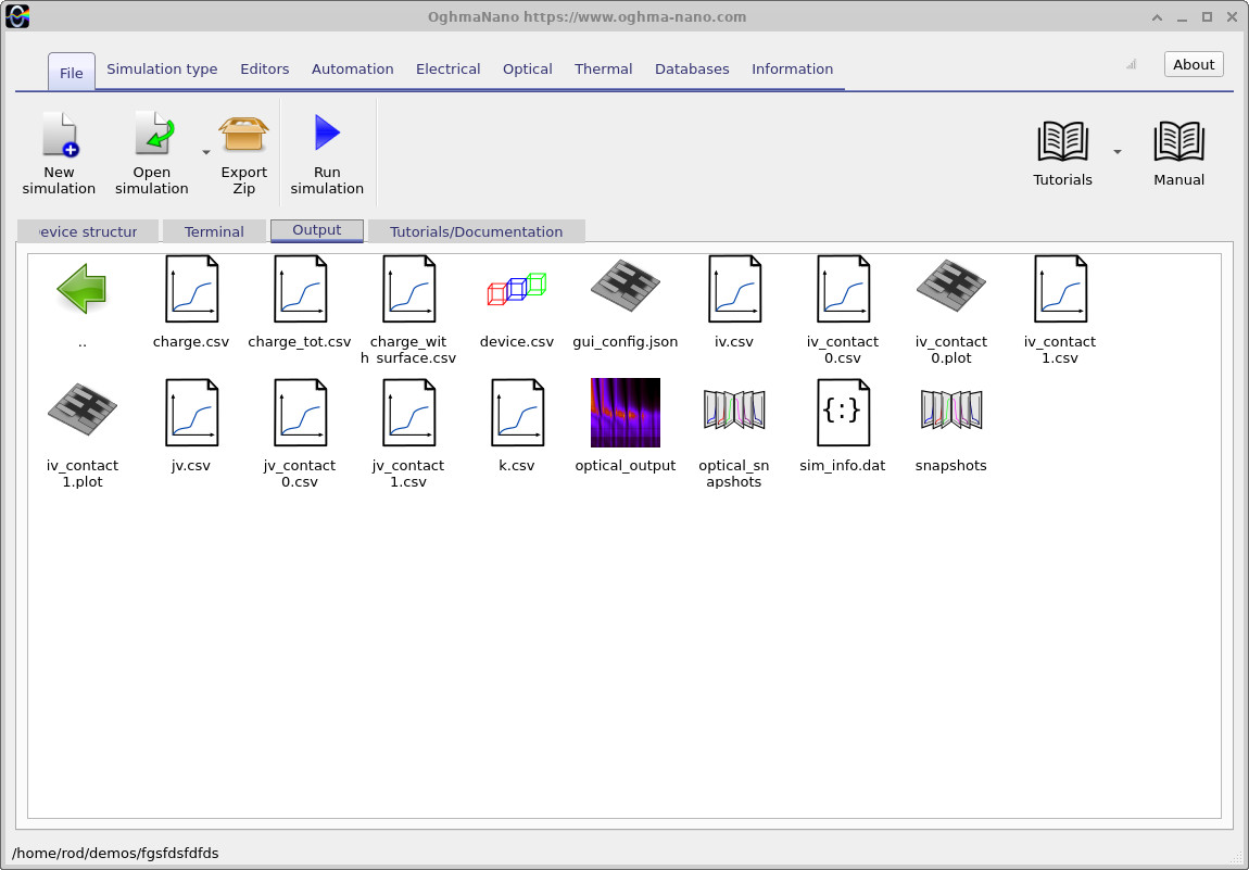
When the calculation finishes, select the Output tab
(??).
OghmaNano writes its results into the simulation directory, including
jv.csv, which contains the J–V curve, and
sim_info.dat, which contains the principal photovoltaic figures
of merit. The optical_output and snapshots directories
contain further information about the optical and electrical behaviour.
See the output files documentation
for additional details.
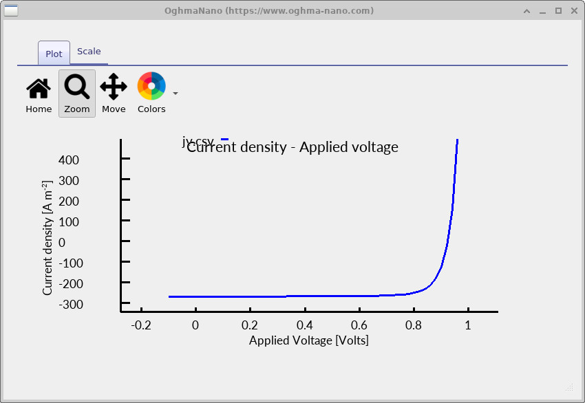
Double-click jv.csv to display the illuminated J–V curve
(??).
The current remains approximately constant under reverse bias and small forward
bias, before increasing rapidly as the applied voltage approaches the
open-circuit voltage. Double-click sim_info.dat to examine the
extracted device performance
(??).
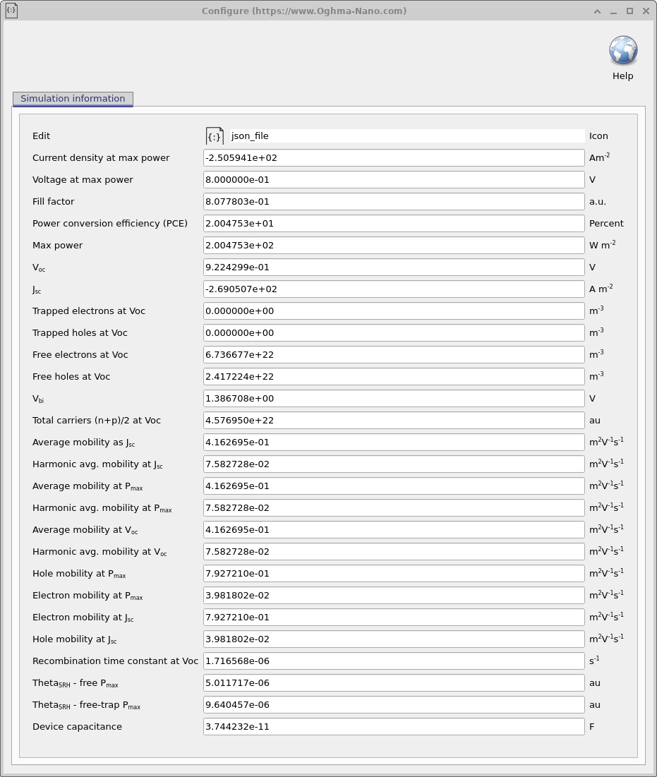
The key results from the GaAs/AlGaAs solar-cell simulation are summarised below.
| Quantity | Value |
|---|---|
| Short-circuit current density, JSC | −269.05 A m⁻² (−26.91 mA cm⁻²) |
| Open-circuit voltage, VOC | 0.9224 V |
| Fill factor, FF | 80.78% |
| Power conversion efficiency, PCE | 20.05% |
| Maximum power density, Pmax | 200.48 W m⁻² |
| Voltage at maximum power, Vmp | 0.800 V |
| Current density at maximum power, Jmp | −250.59 A m⁻² |
| Built-in voltage, Vbi | 1.387 V |
The short-circuit current density, JSC, measures the photocurrent when the applied voltage is zero. Its negative sign reflects the convention that photovoltaic current flows opposite to the forward diode current. The magnitude, approximately 26.9 mA cm⁻², indicates that a substantial fraction of the incident sunlight is converted into collected charge carriers.
The open-circuit voltage, VOC, is the voltage at which the net current becomes zero. Under these conditions, photogeneration is balanced by recombination, and the device can no longer deliver current to an external circuit. The calculated VOC of 0.922 V is lower than the built-in voltage of 1.387 V, reflecting the influence of recombination and the finite carrier populations maintained under illumination. For more information, see calculating the built-in potential.
The fill factor describes how closely the J–V curve approaches an ideal rectangular shape, while the power conversion efficiency gives the fraction of incident optical power converted into electrical power:
\[ \mathrm{FF}=\frac{|J_{mp}|V_{mp}}{|J_{SC}|V_{OC}}, \qquad \mathrm{PCE}=\frac{|J_{mp}|V_{mp}}{P_{in}} \]
For an incident power density of 1000 W m⁻² under AM1.5G illumination, the calculated maximum power density of 200.48 W m⁻² corresponds to a power conversion efficiency of 20.05%. The fill factor of approximately 80.8% indicates that the simulated device maintains a substantial photocurrent over much of its operating voltage range. The maximum power point occurs at approximately 0.80 V. Its precise position depends on the voltage resolution selected in the J–V editor.
The simulated efficiency of approximately 20% demonstrates the high photovoltaic performance achievable with GaAs-based solar cells. The direct bandgap of GaAs enables strong optical absorption, while the AlGaAs window helps reduce optical and recombination losses at the front surface. Further improvements can be achieved by optimising the layer thicknesses, doping concentrations and optical design. For example, adding an anti-reflection coating can increase the fraction of incident sunlight absorbed by the device; see the anti-reflection coating tutorial.
5. Examine the optical simulation

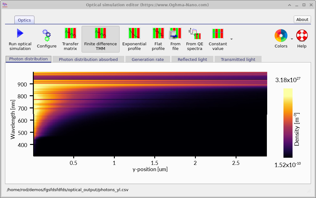
Click the Optical tab at the top of the main window to open the optical ribbon (??). Note that Light intensity (Suns) is set to 1.0. Click Transfer Matrix to open the Optical simulation editor.
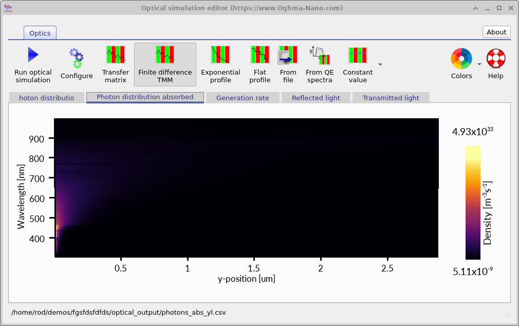
The editor's toolbar lets you choose how the optical generation profile is calculated: Transfer matrix, Finite difference TMM, or simpler profiles (Exponential profile, Flat profile, From file, From QE spectra, Constant value). In this example the highlighted model is Finite difference TMM. Transfer-matrix methods treat the device as a stack of thin films and calculate the forward- and backward-travelling optical fields in each layer, accounting for reflection and interference at every interface and absorption within each layer. Click Run optical simulation to recalculate the optical fields without rerunning the electrical model. For background, see What is the transfer matrix method and the transfer matrix method in OghmaNano. The Photon distribution tab (??) shows the photon density as a function of wavelength and depth, and the Photon distribution absorbed tab (??) shows where those photons are absorbed. The Generation rate, Reflected light and Transmitted light tabs give the integrated generation profile and the reflection and transmission spectra.
Several features are clear in these maps:
- Short wavelengths are absorbed close to the surface. GaAs absorbs blue light very strongly, so these photons are absorbed within the first few hundred nanometres, in the emitter and near the junction.
- Longer wavelengths penetrate deeper and are absorbed throughout the n-GaAs absorber. This is why the absorber needs to be micrometres thick.
- Above roughly 870 nm, photons pass through the whole device without being absorbed. These photons have energies below the GaAs bandgap and cannot generate carriers.
- The dark horizontal lines at certain wavelengths (for example near 760 nm) follow dips in the incident AM1.5G spectrum caused by atmospheric absorption, rather than features of the device.
Every photon absorbed in the GaAs creates an electron–hole pair; this absorbed photon density becomes the generation rate \(G\) in the drift-diffusion equations. The AlGaAs window has a wider bandgap than GaAs, so photons with energies between the two bandgaps pass through it and are absorbed in the GaAs below, where the resulting carriers can be collected. Photons absorbed in the window itself, or in GaAs very close to an unpassivated surface, are much more likely to be lost to recombination.
6. Electrical material parameters
Return to the main window, select the Device structure tab and click Electrical parameters in the left-hand toolbar. This opens the Electrical parameter editor (??), which contains a tab for each semiconductor layer. The screenshot shows the Al0.3Ga0.7As window selected, with the general AlxGa1-xAs Lua material model displayed in the Code editor. The aluminium fraction \(x\) is controlled through the Gradients/Strain editor (??). The toolbar also controls the electrical physics: drift–diffusion and equilibrium Shockley–Read–Hall (SRH) traps are enabled, while dynamic traps, Auger recombination and exciton transport are disabled. The latter models are particularly useful for certain disordered semiconductor devices but are not required here.
OghmaNano allows material properties to be specified directly or calculated using its materials database. For well-characterised inorganic semiconductors such as GaAs, AlGaAs and InGaAs, the database provides models for properties such as bandgap, electron affinity, carrier mobility and recombination, including their dependence on composition and temperature. These models are implemented as Lua scripts, with available materials listed in the Lua material model library. When the Script button is pressed, the simulator uses the selected Lua material model. When it is not pressed, the simulator instead uses values entered directly into the Parameters tab. This simpler approach is particularly useful for disordered or less well-characterised semiconductors, where material parameters are often varied independently.
The two approaches can also be combined, as illustrated in the Parameters tab (??). Here, properties such as carrier mobility, effective densities of states, bandgap and electron affinity are entered directly, while others, including the SRH trap parameters, are supplied by the Lua model and marked See script for value. To control this behaviour, click the arrow beside Script and select Override materials DB (??). Ticked parameters use the values in the text boxes, while unticked parameters use the material database. This is useful for investigating heterojunction band offsets or varying individual parameters without modifying the underlying material model. The same menu also contains Import material script, allowing a different Lua model to be selected from the database.
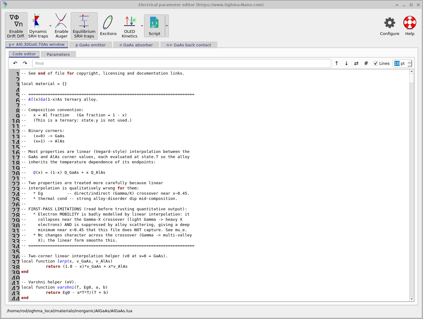
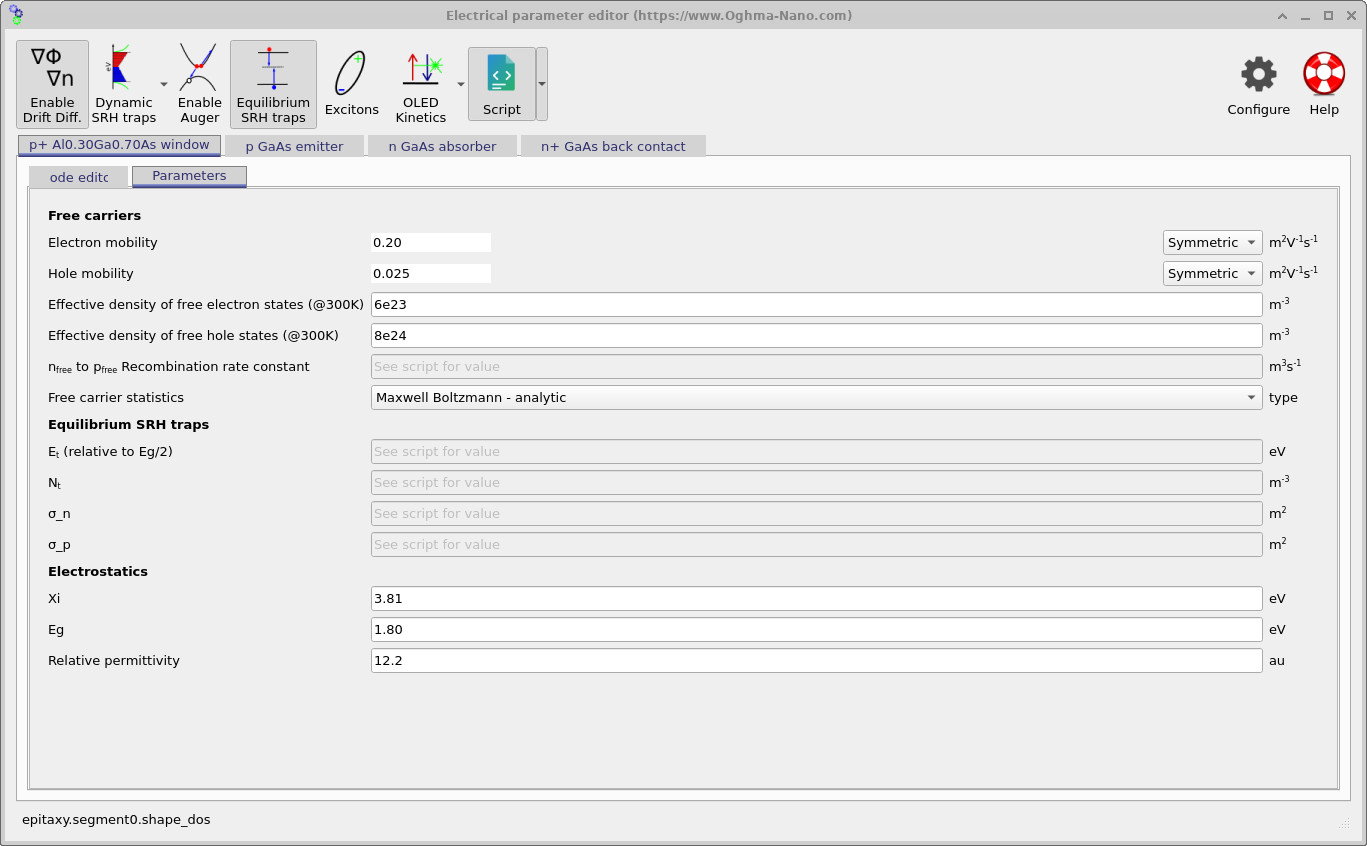
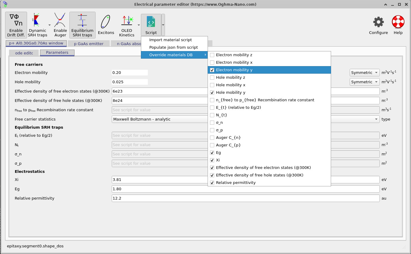
In this example, the y-direction electron and hole mobilities, bandgap, electron affinity, effective densities of states and relative permittivity are overridden, while recombination parameters continue to come from the Lua model. This is useful when investigating heterojunction band alignment, since changing the bandgap or electron affinity allows conduction- and valence-band offsets to be varied without modifying the shared material database. Overrides can also be used for parameter sweeps and comparisons with experimental data.
The Script menu also provides an Import material script option for selecting another material model from the database. For more information, see defining electrical parameters with Lua, the materials model library and the materials database documentation. User-specific material definitions are stored in oghma_local.
💡 Tip: Overridden parameters no longer follow the material script. For example, overriding the AlGaAs bandgap means that changing the aluminium fraction will not change its value. Untick the override to restore the composition dependence.
7. Energy bands and quasi-Fermi levels
One of the most useful tools for understanding a semiconductor device is the
snapshot viewer. This allows quantities such as the energy
bands, carrier densities and electric fields to be plotted at different
steps during a simulation. For example, during a J–V sweep, the viewer
shows how these quantities change with applied voltage, while in a transient
simulation it shows their evolution with time. To open the viewer, go to
the Output tab and double-click the snapshots folder.
The slider at the bottom of the window allows you to move between simulation
steps. See the snapshot viewer documentation
for more information.
An interesting starting point is to compare the device in the dark and under illumination. To simulate the device in the dark, select the Optical ribbon and set Light intensity (Suns) to zero (??), then rerun the simulation. The resulting energy-band diagram at approximately 0 V is shown in ??. Notice that the electron and hole Fermi levels coincide and are completely flat across the device. This is characteristic of thermal equilibrium: although the semiconductor bands bend considerably, there is no net current flowing through the device.
Now restore the illumination to 1 Sun and rerun the simulation. The corresponding band diagram at approximately 0 V is shown in ??. The conduction and valence bands remain similar to those in the dark, but the electron and hole quasi-Fermi levels are no longer coincident. Instead, they separate as photogenerated electrons and holes establish non-equilibrium carrier populations within the device.
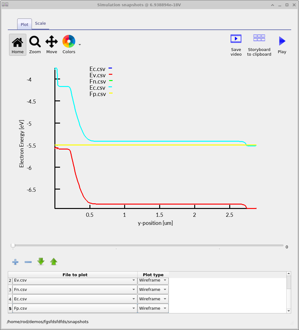
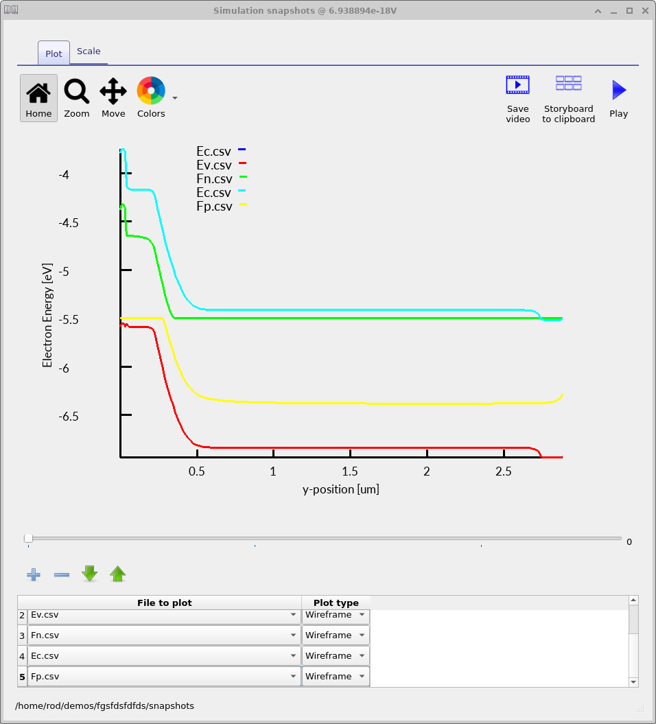
Looking more closely at the band diagrams, the most prominent feature is the strong band bending between approximately 0.25 µm and 0.55 µm. This corresponds to the depletion region of the GaAs p–n junction. Because the n-type absorber is more lightly doped than the p-type emitter, the depletion region extends predominantly into the absorber. The resulting built-in electric field helps separate photogenerated electron–hole pairs, driving electrons towards the n-type contact and holes towards the p-type contact.
Another interesting feature appears at the illuminated surface, where the AlGaAs window meets the GaAs emitter. The discontinuity in the conduction band arises from the different electron affinities and bandgaps of the two materials. This heterojunction creates an energy barrier that helps prevent minority electrons in the p-type emitter from reaching the front surface, where they could recombine. A smaller change is also visible near the rear of the device, corresponding to the transition into the heavily doped n+ contact layer.
The separation between the electron and hole quasi-Fermi levels provides a measure of how far the semiconductor is from equilibrium. For non-degenerate carrier statistics, the local electron and hole populations are related to this separation by
\[ np = n_i^2 \exp\left(\frac{E_{F,n}-E_{F,p}}{k_B T}\right) \]
Under illumination, photogeneration increases the carrier populations and produces a splitting between \(E_{F,n}\) and \(E_{F,p}\). This splitting can exist inside the device even at short circuit, where the externally applied voltage is zero. At open circuit, the terminal voltage is determined by the quasi-Fermi-level separation established at the contacts, with \(qV_{OC}\) corresponding to that separation for ideal selective contacts. Recombination limits how large this splitting can become and therefore plays a central role in determining the open-circuit voltage. By moving through the voltage sweep using the snapshot slider, you can observe how the energy bands and quasi-Fermi levels evolve as the solar cell approaches VOC.
9. Further investigations
🧪 Try it yourself: Now that you understand the operation of the GaAs/AlGaAs solar cell, try the following investigations. Each can be performed manually or automated using an OghmaNano parameter scan. Before expanding the answers, try to predict how each change will affect the J–V curve and photovoltaic efficiency.
-
🔬 Task 1: Change the aluminium fraction in the AlGaAs window. What happens to the solar-cell performance as the aluminium fraction \(x\) increases?
Show expected result
Increasing the aluminium fraction increases the AlGaAs bandgap, making the window more transparent to incident sunlight. It also changes the conduction- and valence-band offsets at the AlGaAs/GaAs interface, potentially reducing surface recombination but also affecting carrier extraction. The optimum composition is therefore a compromise between optical transmission and electrical transport. Remember to disable any parameter overrides that would prevent the Lua model from responding to changes in composition.
-
📏 Task 2: Change the thickness of the AlGaAs window. Does making the window thinner improve the short-circuit current?
Show expected result
A thinner window generally reduces unwanted absorption of short-wavelength photons, allowing more light to reach the underlying GaAs emitter and absorber. This may increase JSC. However, the window also influences the electrical properties of the front contact region, so reducing its thickness indefinitely is not necessarily beneficial. Examine both the J–V curve and the optical absorption profile.
-
⚡ Task 3: Vary the emitter and absorber doping concentrations. How does doping affect VOC, JSC and the depletion region?
Show expected result
Changing the doping modifies the built-in potential, depletion-region width and electric-field distribution. Increasing doping generally narrows the depletion region and changes the carrier concentrations, which can influence both collection and recombination. Higher doping does not necessarily produce a better solar cell: the optimum depends on the balance between carrier extraction, conductivity and recombination losses.
-
☀️ Task 4: Change the thickness of the GaAs absorber. What happens when the absorber becomes thinner or thicker?
Show expected result
Increasing the absorber thickness allows more photons, particularly at wavelengths approaching the GaAs absorption edge, to be absorbed. This can increase JSC. However, photogenerated carriers must travel further to reach the contacts, increasing the opportunity for recombination. Eventually, additional thickness provides little optical benefit and may reduce electrical performance.
-
🔄 Task 5: Increase the SRH trap density. How does stronger non-radiative recombination affect the J–V curve?
Show expected result
Increasing the trap density or carrier capture cross-sections generally increases SRH recombination. This reduces the carrier lifetime and the quasi-Fermi-level splitting under illumination, leading to a lower VOC. Stronger recombination may also reduce JSC and the fill factor. Compare the J–V curves before and after changing the trap parameters.
-
🔍 Task 6: Replace the AlGaAs window with GaAs. Does the heterojunction improve the performance compared with a GaAs homojunction?
Show expected result
Replacing AlGaAs with GaAs removes the wider-bandgap window and its associated band offsets. This changes both the optical absorption profile and minority-carrier transport near the illuminated surface. Depending on the surface recombination parameters, the absence of the window may increase recombination losses and reduce efficiency. Compare the resulting J–V curves and band diagrams. The GaAs PN junction tutorial provides a useful introduction to homojunction behaviour.
-
📉 Task 7: Investigate the heterojunction band offsets. What happens when you change the bandgap or electron affinity of the AlGaAs window?
Show expected result
The bandgap and electron affinity determine the conduction- and valence-band discontinuities at the AlGaAs/GaAs interface. Changing these parameters alters the energy barriers experienced by electrons and holes. A suitable conduction-band barrier can suppress minority-electron transport towards the front surface, while an excessively large valence-band barrier may impede hole extraction and reduce the fill factor. Use the Override materials DB option to investigate these effects independently of the Lua model.
10. Summary and what you have learned
In this tutorial, we have simulated a GaAs/Al0.3Ga0.7As heterojunction solar cell, consisting of a wide-bandgap AlGaAs window, a p-type GaAs emitter, an n-type GaAs absorber and a heavily doped back contact. Under one-Sun illumination, the simulation gives a short-circuit current density of 26.91 mA cm⁻², an open-circuit voltage of 0.922 V, a fill factor of 80.8% and a power conversion efficiency of 20.05%. These results demonstrate how the optical and electrical properties of a semiconductor heterostructure combine to determine its photovoltaic performance.
By examining the optical generation profiles and energy-band diagrams, we have seen how sunlight is absorbed within the GaAs layers, how the built-in electric field separates photogenerated carriers, and how the AlGaAs/GaAs heterojunction introduces band offsets that influence carrier transport and recombination. Comparing the device in the dark and under illumination also demonstrated the importance of quasi-Fermi-level splitting and its relationship to the open-circuit voltage.
Finally, we explored how OghmaNano combines optical transfer-matrix calculations with drift–diffusion modelling, and how its Lua materials database and parameter override system allow semiconductor properties to be controlled. Together, these tools provide a framework for investigating how layer thickness, doping, alloy composition and material properties influence device performance. The same approach can be extended to other III–V photovoltaic devices and semiconductor heterostructures.
👉 Next steps:
- Work through the investigations in Section 9, changing one parameter at a time and recording JSC, VOC, FF and PCE.
- The same approach — layered device, Lua material models, overrides and coupled optical and electrical simulation — extends to other III–V devices, such as photodiodes, other heterojunction cells and multi-junction structures.
- Continue with the GaAs 3D drift–diffusion series, starting with GaAs 3D drift–diffusion with a vertical defect, or browse the other GaAs device examples.
- For a broader overview of inorganic device modelling, see silicon and semiconductor device simulation.